
Submitted:
02 October 2024
Posted:
02 October 2024
You are already at the latest version
Abstract
This study presents a synthesizer topology based on a DLL and programmable frequency multiplier for 5G+ communication systems. The proposed synthesizer comprises a 512-phase DLL, an intermediate frequency generator (IFG), and an RF frequency multiplier (RFFM). The 512-phase DLL provides 512 delayed pulses through a chain of 256 delay units and single-to-differential complementary converters (S2DCs). The IFG comprises I/Q-multiplexers, I/Q-accumulators, an XOR, and an S2DC. The I/Q-multiplexer outputs switch to the phase lag or lead waveforms at every rising or falling edge of the outputs, which makes the I/Q-multiplexer output frequency, fMX, programmable. The IF, fIF, is two times fMX, and fIF is up-converted to RF, fRF, through the RFFM. When reference clock frequency, fref is 156.25 MHz, the fIF range is 156.863–312.5 MHz and the fRF dynamic range is approximately 1.89–9.96 GHz. The channel resolution range is 3.698–38.609 MHz. Consequently, the proposed synthesizer provides a wide 134 % output frequency bandwidth and a finer channel resolution smaller than fref. The presented synthesizer is fabricated in a 65-nm CMOS process. The total power consumption is 15 mW, and the rms jitter integrated from 12 kHz to 20 MHz measured as 83 fs.
Keywords:
5G synthesizer
; CMOS integrated circuits
; delay-locked loop (DLL)
; harmonic suppression
; integrated rms jitter
; programmable frequency multiplier
; phase locked loop (PLL)
1. Introduction
The quality factors of inductor (L) and capacitor (C) are small at the millimeter wave (mmWave). Therefore, designing an ultra-low phase noise (PN) LC voltage-controlled oscillator (VCO) that adheres to the stringent integrated jitter specification for the beyond 5G communication systems is tough. The cascade local oscillator (LO) generator structures of a lower-frequency synthesizer and a frequency multiplier (FM) have been recently published [1,2,3,4,5] to accomplish the jitter performance. The main goals of the lower-frequency synthesizer are to provide the best in-band phase noise (PN) and the finest channel resolution performances.
A multiplying delay-locked loop (MDLL), a subsampling phase-locked loop (SSPLL), and an injection-locked PLL (ILPLL) are good candidate topologies to achieve ultra-low in-band PN. Figure 1(a) shows a phase edge combined (EC)-based MDLL block diagram. Output frequency (fout) can be expressed as N×fin/2, where N is an even integer number of delay cells in a voltage-controlled delay line (VCDL). Therefore, the MDLL channel resolution would be fin. The biggest advantage of the MDLL is that it is free from jitter accumulation, which will improve the in-band PN. However, N is strictly difficult to program because the delay unit number in a VCDL must be changed. Therefore, its channel programmability is limited [6,7,8,9].
Both the SSPLL and ILPLL (Figure 1(b) and Figure 1(c)) have the same channel resolution (fin) but require extra frequency tracking loops (FTLs) for locking the output frequency as N×fin. After the target frequencies are tuned, the FTLs are turned off, and their lock states are maintained by a subsampling phase detector (SSPD) for the SSPLL and cascade connection of a digitally-controlled delay line (DCDL) and a pulse width controller for the ILPLL. Therefore, their in-band PNs will be improved because in-band PN sources are no longer multiplied by N2 when transferred to the PLL outputs [10,11,12]. However, neither the SSPLL nor the ILPLL is suitable for high-magnitude multiplication, N, because it is difficult to design a reliable SSPD and DCDL as N is increased [13,14,15,16]. Consequently, the number of possible programmable channels is also restricted.
This paper presents a new cascade topology of a DLL-based synthesizer and an FM for a lower-frequency synthesizer. The DLL-based synthesizer consists of a 512-phase DLL and an intermediate frequency generator (IFG), providing a wide IF band. The IF band is up-converted to the RF band by the programmable high-frequency multiplication factor (FMF) RFFM. Therefore, the proposed synthesizer can provide ultra-low in-band PN, a channel resolution that is finer than the input frequency (fin), ultra-low out-band PN, and a wide frequency band. The proposed synthesizer is fabricated in a 65-nm CMOS process, and the active die area is 0.6 mm2. The total power consumption is 15 mW without counting a 50 Ω driving amplifier (DA) power consumption. Recent 5G LO research papers have achieved their rms jitter performances while using signal generators as reference clocks. However, our main purpose is to implement the optimum LO module solution for 5G+ wireless communication systems composed of the proposed synthesizer and currently available state-of-the-art reference external oscillators. When a 156.25 MHz micro-electro-mechanical systems (MEMS) differential oscillator (SiT9501) is applied as the reference clock, the LO module output frequency range is 1.88–9.96 GHz, and its channel resolution range is 3.698–38.609 MHz. The integrated rms jitter from 12 kHz to 20 MHz is 83 fs.
The rest of this paper is organized as follows: In section II, a new synthesizer topology is introduced. Its components are explained as well as their functionalities. Then, the proposed synthesizer output frequency range and channel resolution equations are presented. Finally, the synthesizer’s phase noise analysis and the benefits are presented. Section III shows core building block schematics. The core circuitries are analyzed and verified through simulations. Also, the design procedure for the target output frequency range is talked about in detail. Furthermore, the synthesizer’s adjacent harmonic rejection ratio analysis and simulation are presented last. The proposed synthesizer chip fabrication and printed circuit board (PCB) environment for testing the chip are shown in Section IV. Moreover, the synthesizer’s power consumption is summarized, and the DA output matching and capacitor bank (Cbank) calibration are discussed. Finally, the test measurements of core specifications are reported. The summary and comparative analysis with recently published synthesizers are presented in Section V.
2. Topology, Analysis, And Frequency Range
2.1. Synthesizer Topology, RF Range, and Channel Resolution
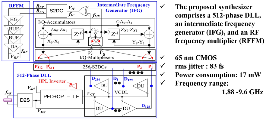
The proposed synthesizer consists of three subsidiary blocks (blue-color boxes): a 512-phase DLL, an IFG, and an RFFM as shown in Figure 2. In terms of functionality, the synthesizer can be divided into two blocks. One is an IF synthesizer consisting of the 512-phase DLL and IFG, and the other is a programmable RFFM.
The DLL’s components are a differential-to-single (D2S) buffer, a phase frequency detector (PFD), a charge pump (CP), a loop filter, a voltage-controlled delay line (VCDL), and 256-phase single-to-differential complementary converters (256-S2DCs). The external oscillator frequency is denoted by fref, and its differential outputs are converted to VMS through the D2S. The frequency of VMS is fMS (= fref), driving the PFD and VCDL. And, the VCDL is composed of a cascade chain of 256 delay units (DUs). An inverter (red) is inserted at the VCDL output to make it half-period locked, and its output (Vdel) is fed to the other PFD input. The phase difference between VMS and Vdel is manipulated by the PFD+CP, which adjusts VCT to control the delay of all the DUs simultaneously. When the phases of VMS and Vdel are locked, Vdel is delayed by TMS/2 from the rising edge of VMS, where TMS (= 1/fMS) is the period of VMS. Therefore, each DU’s delay, td, is uniformly equal to TMS/512. An S2DC comprises two XORs: one XOR input is connected to a power supply, and the other XOR input is connected to a ground as shown in the dotted box of Figure 3(a). Figure 3(b) shows that the 256 different phase (D1–D256) pulses are expanded to 512 different phase (P1–P512) pulses through the 256-S2DCs.
The IFG consists of I/Q-multiplexers, I/Q-accumulators, an XOR, and an S2DC. All digital bits of A9–A1, Zy9–Zy1, and Zx9–Zx1 are programmable. After the DLL is locked, the accumulators add or subtract the input magnitude (A9–A1) from the previous values (Zy9–Zy1 or Zx9–Zx1). Depending on the accumulator output state of Y9–Y1 (or X9–X1), VQ (or VI) is switched to the PM multiplexer input, where M is equal to the magnitude of Y9–Y1 (or X9–X1). For example, when the magnitude of Y9–Y1 = 1, VQ is connected to P1. VQ and VI drive the I/Q-accumulator’s D-flip-flops (DFFs) and XOR gate of generating VIF. Depending on a feedback clock control (CFC) state, VQ (or VI) is connected to either the left or right accumulator’s DFF. By applying the appropriate initial states of Zy9–Zy1 and Zx9–Zx1, the time delay between VQ and VI can be either TMX/4 or (TMX/4)–td. TMX is the VQ (or VI) pulse period. The consequent VIF’s fundamental frequency (fIF) = 2×fMX, where fMX = 1/TMX.
To visualize simple examples of how to vary fIF, the multiplexer input phases are set to 16. As shown in Figure 4(a), P1–P16 waveforms are uniformly delayed by td (= TMS/16). When the magnitude (ACM) of A9–A1 is programmed as 6, and VQ (or VI) is switched to the phase lead signal at its rising and falling edges, the shift of VQ (or VI) would follow as the sequence P16, P10, P4, P14, P8, P2, P12, P6, and P16. By combining the sequence, the high and low state durations of VQ are reduced by 6td, which results in a 50% duty cycle 4td period pulse as indicated by the purple pulse at the bottom of Figure 4(a).
Unlike the previous phase shift pattern, VQ and VI might be switched to the phase lag signal. In addition, VQ might be updated by VI, and VI might be updated by VQ. Figure 4(a) shows VQ and VI shift sequences (blue and red) when ACM = 1. Initially, VI and VQ are connected to P7 and P10. VQ is switched to P11 at the first rising edge of VI, while VI is switched to P8 at the first rising edge of VQ. The second phase shift of VQ from P11 to P12 happens at the first falling edge of VI. Moreover, VI is switched to P9 at the first falling edge of VQ. By continuously updating in the just mentioned method, the phase shift sequence of VI (VQ) would be P7 (P10), P8 (P11), P9 (P12), P10 (P13), and P11 (P14). The final pulses of VI and VQ are 50% of the duty cycle and their period would be 18td because high and low state durations are increased to 9td at each rising and falling edge from 8td.
Figure 4 (b) shows all waveforms of VQ and VI for ACM = 2, 3, 4, 5, and 6 when VQ and VI are shifted to the phase lag signal. The waveforms of VQ and VI shifting to the phase lead signal waveforms for ACM = 1, 2, 3, 4, and 5 are shown in Figure 4(c). All VQ and VI waveforms are 50% duty cycle pulses. However, VIFs are 50% duty cycle pulses (Figure 5(a)) when the period of VQ and VI (TMX) is 4td, 8td, 12td, 16td, 20td, 24td, and 28td. Otherwise, the duty cycle (Dcycle) of VIF would be expressed as
as shown in Figure 5(b). If td is reduced and TMX is increased, the duty cycle offset (td/TMX) would be close to zero.
Considering the previous example (P1–P16), TMX would be td × (512±2ACM). Because TMS = 512×td, TMS/TMX can be expressed as 512/(512±2ACM). Therefore, fIF can be derived as
where ACM can be programmed to any integer between 0-254. The proposed synthesizer output frequency can be expressed as
where RFFMF is the RFFM’s FMF. Replacing ACM as ACM+1 in (3) and subtracting it from (3), RF channel resolution (ΔfRF) between ACM and ACM + 1 is expressed as
The ΔfRF would be finer as the denominator of (4) is increased.
Applying fMS = 156.25 MHz for ACM = 1–254, the fIF range is simulated as 156.86–311.28 MHz when VI (VQ) switches to the phase lag pulse. For VI (VQ) shifting to the phase lead pulse, the fIF span will range from 313.73 MHz to 40 GHz. However, fIF is intentionally limited to 311.28 MHz for a fine channel resolution in this paper. RFFMF can be programmed as any even number among 12-32. By setting RFFMF = 32 and ACM = 1, fRF will be 9.96 GHz. A 1.88 GHz fRF can be generated by programming RFFMF = 12 and ACM = 254. The consequent ΔfRF range is 3.698 -38.609 MHz according to (4).
2.2. Phase Noise Analysis and no Jitter Accumulation
The proposed synthesizer PN sources are shown in Figure 6, where θXO, θPC, and θDL are the PN spectral densities (PNSDs) of the reference clock, the PFD+CP, and the VCDL, respectively. KPC (= Icp/(CLS)) and KDL are the PFD+CP and VCDL gains. KSYN is the total FMF from fref (= fMS) to fRF as shown in Figure 2. TMS (= 1/fMS) is much less than the DLL time constant such that exp(-STMS) = 1 [17]. Therefore, the proposed synthesizer output PNSD, θSYN, can be derived as
where
According to (5), the proposed synthesizer has no low-pass filter effect on θXO. Therefore, the integrated rms jitter of θXO should be less than the target jitter such as 100 fs from 12 kHz to 20 MHz of the 28 GHz carrier frequency [18]. The target 100 fs integrated rms jitter is translated as 0.005625˚ at a 156.25 MHz crystal oscillator, which was stringent to achieve a decade ago. Fortunately, ultra-low jitter oscillator products have been recently released with a few hundred frequency range MHz. For example, SiT9501 yields a 70.629 fs rms jitter integrating a 12 kHz–20 MHz offset bandwidth when the operation frequency is 156.25 MHz.
As noted in (6), the noise transfer function (NTF) of the θPC, Hl(S), is a low-pass filter (LPF). Unlike other synthesizers such as the CPPLL, SSPLL, and ILPLL, both values of Icp and CL can be freely selected because the presented DLL has no stability constraint. Therefore, the effect of θPC on the presented synthesizer output can be minimized by manipulating Icp and CL as much as possible. On the contrary, Hh(S), the NTF of θDL is a high-pass filter (HPF) so that lower-frequency PN sources such as flicker noise would be filtered out.
While VCO output jitters in all other PLLs are accumulated until they are fixed by the reference clock as shown in Figure 7, the proposed synthesizer has no jitter accumulation because of no oscillator. Furthermore, a good design FM output’s integrated jitter would be close to the input jitter. In contrast, a typical synthesizer’s integrated jitter is severely degraded by a VCO out-band PN, particularly, for wide data bands.
The absence of a loop stability constraint and VCO makes the proposed synthesizer provide a relatively wide output frequency range, comparable jitter, and a finer channel resolution than fref, compared with the state-of-the-art synthesizers proposed in recently published papers [19,20,21,22,23] and [28].
3. Design of the Proposed Synthesizer and Spur Analysis
3.1. Low Phase Noise PFD and CP
To operate a high-frequency phase synchronization, a true single-phase clocking (TSPC)-based PFD is implemented (Figure 8). Following the PN optimization design procedure described in [24], a small 40 ps on-time (TL) is confirmed by simulations when 156.25 MHz input signals are locked.
Figure 9 shows the presented CP schematic with noise sources, which is the same topology described in [25]; however, BJTs are replaced by CMOS transistors. All channel current noises are included but all flicker voltage noises at the transistor (M1–M5) gates are omitted for simplicity. Because Mn and Mp are used for switches, their noise contributions are trivial. Most of the noises due to M3–M5 are filtered by RG1–CG1 and RG2–CG2 LPFs. The current noises of M1 and M2, and can be degenerated by Rdn and Rdp, respectively. However, some portions of Rdn and Rdp noises are added. Therefore, the equivalent current noise () flowing through the M1 channel is expressed as
According to (7), the equivalent current noise would be close to 4kT/Rdn if Rdngm1 is big enough. As Rdn is increased, is decreased. Therefore, the maximum possible Rdn must be used to minimize the equivalent current noise as long as guarantees an appropriate output tuning DC range.
To secure the degeneration Rdn benefit, should be less than , which can be expressed as
When Rdngm1 >> 1, (8) can be simplified as
which defines the minimum required degeneration resistance to reduce the CP output noise due to .
Moreover, the flicker noises of M1 and M2, and, can be individually alleviated by gm1Rdn and gm2Rdp. Consequently, the equivalent output current noise, , can be expressed as
where
Figure 10 shows the PN simulations of the PFD+CP when the degeneration resistance (both magnitude of Rdn and Rpn) is 62.5, 125, 250, 500, 1k, 2k, and 4k ohm. The smallest simulated PN at 1 kHz offset is –135 dBc/Hz which is 21 dB lower than that of SiT9501. However, the lowest PN at 10 kHz offset is –141dBc/Hz, which is close to that of SiT9501. Therefore, the DLL 3-dB loop bandwidth must be lower than 10 kHz to force the dominant in-band PN source for the proposed synthesizer to be the external reference clock. The best PN floor is -143 dBc/Hz.
3.2. Delay Unit
As shown in Figure 2, the VCDL is the chain of 256 DU cells. Each DU output drives DU input, but the last DU drives the inverter for a half-period lock. Therefore, to make all nodes (D1–D256) an identical capacitive load, the last DU should be different from the other DUs.
The DU schematic shown in Figure 11(a) is used for the first 255 DUs in the chain, which consists of two delay unit inverters (IDUs), two varactors (Vars), and two 3-bit Cbanks. The DU output drives the multiplexer through the inverter buffer (IB). Adding a dummy buffer inverter (IB) at the DUX node makes the same capacitive load for the DUX and DUout nodes. In addition, another dummy inverter (IH) is applied to both DUX and DUout nodes, where IH is the last DU’s load inverter for the half-period lock shown in Figure 2. Figure 11(b) shows the last DU schematic. The only difference is that the dummy inverter (IH) is replaced by IDU at the DUout node. Consequently, all nodes of the DU inverter (IDU) in the VCDL have the same capacitive load, which leads to the same delay for each DU inverter. The reason for the 3-bit Cbank is to reduce KDL to make the DU less sensitive to the power supply and delay line noises as well as to minimize the DU PN.
The delay, DT, from DUin to DUout, can be varied by adjusting the capacitance of Var, which is inversely proportional to the VCT magnitude. Figure 12 shows the simulated DT versus VCT when two extreme process/temperature variations of FF/–20 ºC and SS/100 ºC are applied. The delay curves of FF/–20 ºC (blue) and SS/100 ºC (red) should be overlapped to overcome the variations of the ±3σ process and the −20 to 100 ˚C temperature range. The overlapped delay must include TMS/512 to make DLL locked, which would be 12.5 ps when fMS = 156.25 MHz. The VCT node would converge to either 1.2 V or 0.9 V for both FF/-20 ºC/ ‘111’ Cbank state and SS/100 ºC/ ‘000’ Cbank state, respectively.
The DU chain PN simulations on DU16, DU32, DU48, DU64, and DU80 outputs have been completed, as shown in Figure 13 (blue curves). Beyond the DU80 output, PN simulation cannot be accomplished owing to the convergence problem in Cadence. Therefore, PN beyond the DU80 output is induced by linearly expanding from the PN simulations on DU16, DU32, DU48, DU64, and DU80 outputs. The average PN degradations between DUX+16 and DUX outputs for flicker and thermal noise regions are 1 and 0.25 dB, respectively. As a result of expansion, PN degradations of approximately 11 and 2.75 dB are estimated between DU256 and DU80 outputs (the red curve in Figure 13).
The PN contribution of S2DC (Figure 3) is trivial so the PN on P512 is close to that on DU256. Because VQ or VI in Figure 2 is continuously switched among P1–P512, the average PN on either VQ or VI is always better than that on P512. Rather, the average PN for all possible pulses programming A9–A1 would be close to the PN on P128, where the estimated PN on P128 is approximately equal to 3 dB and 0.75 dB PN degradations from the P80 PN as shown in the black curve in Figure 13.
To prove the above statement, the jitter-added P1–P16 pulses on rising and falling edges are shown in Figure 14(a). The single DU’s jitter (J1) is added on P1. The jitter on P2 would be double as 2Jt, and 15Jt will be accumulated finally on P15. However, the jitter on P16 is fixed by PFD+CP such that no jitter exists on P16. For A4–A1 = 1, the period of VIF is adjusted to 9td (the bottom in Figure 14(b)). The accumulated jitter at the rising edge of VIF is varied as the sequence of 7Jt, 8Jt, 9Jt, 10Jt, 11Jt, 12Jt, 13Jt, 14Jt, 15Jt, 0, Jt, 2Jt, 3Jt, 4Jt, 5Jt, and 6Jt. Moreover, the accumulated jitter at the falling edge of VIF is varied as the sequence of 11Jt, 12Jt, 13Jt, 14Jt, 15Jt, 0, Jt, 2Jt, 3Jt, 4Jt, 5Jt, 6Jt, 7Jt, 8Jt, 9Jt, and 10Jt. Therefore, the average jitter at both rising and falling edges of VIF would be 8Jt. When A4–A1 = 6 (the 14td period waveform in Figure 14(b)), the accumulated jitter sequence at the rising edge of VIF would be 7Jt, 13Jt, 3Jt, 9Jt, 15Jt, 5Jt, 11Jt, and Jt. The jitter sequence at the falling edge of VIF would be 14Jt, 4Jt, 10Jt, 0, 6Jt, 12Jt, 2Jt, and 8Jt. The resulting accumulated average jitter would be 8Jt and 7Jt at the rising and falling edges of VIF, respectively.
3.3. Programmable RFFM
As shown in Figure 2, RFFM is composed of an HG, two buffers (BUFs), and a drive amplifier (DA). The proposed HG schematic is shown in Figure 15, which has been recently published in [25,26]. [26] has implemented it as a frequency quadrupler and [25] has applied it as a programmable FM for 8–16 FMF range. The HG in this paper has been optimized for the programmable 12–32 FMF range.
All the transistors of M1–M6 in Figure 15 are fully turned on and off periodically by applying enough amplitude at (TP–TN). Figure 16(a) shows the ideal HG’s important internal voltage and current pulses. The corresponding output currents are illustrated in Figure 16(b). The delay time (Tw) between the differential signals of (TP–TN) and (BP–BN) is intentionally introduced by adjusting Cs and Cg. The current (IM4) flows only for the duration of both TN and BN in the high state. Because IM1 = IM3 + IM4, the high state pulse width of IM3 is Tw but that of IM4 is TIF /2 – Tw, where TIF = 1/fIF. Similarly, IM5 and IM6 can be generated by applying the complementary pulses (TP and BP) of (TN and BN). The fundamental frequency of IM3–IM6 is still fIN (= 1/TIN), but their summation (IHG+ and IHG-) fundamental frequency is 2×fIN. Figure 16(b) shows the HG differential current (IHG+ − IHG-) pulse (purple), which would provide strong even current harmonics.
According to (2), fIF is equal to fMS×(1024/1020) by programming ACM as 254. Since fMS is 1/(512×td), the corresponding period of VIF would be 510×td. When td is 12.5-ps, the VIF period is 6.375-ns and the period of (IHG+ − IHG-) is 3.1875-ns. Figure 17(a) shows the 3.1875-ns fundamental period pulse with a 20-ps pulse width, 20-ps rising delay, and 20-ps falling delay. Its power spectrum is also shown in Figure 17(b). The power difference between 0.3137 and 10.04 GHz is only 2.8 dB, which means that the power is more balanced and distributed over a 0.3–10 GHz frequency band compared with a 50 % duty cycle pulse.
Unfortunately, the ideal current pulse of the above example cannot be produced because all active devices have limited bandwidth. Instead, it is more likely to draw the differential output current (IHP+ − IHP-) as shown in Figure 17(c), which is the simulation result when ACM is set to 254. Figure 17(d) shows the Fourier transform of (IHP+ − IHP-). Because of the slew rate, the low-order harmonic characteristic would be expressed as highlighted with the purple dotted ellipse, which leads to more power concentration on 2×fIF, 4×fIF, and 6×fIF. Consequently, the power spectrum difference between those at the lowest and the highest harmonics is now 10.2 dB, which is 7.4 dB bigger than that of the ideal (IHP+ − IHP-) spectrum. However, the power spectrum difference between those at 1.882 and 10.04 GHz is 2.9 dB, which is only 0.2 dB bigger than that of the ideal pulse (2.7 dB power difference between those at 1.882 GHz and 10.04 GHz as shown in Figure 17(b)). As shown in Figure 15, the wanted high-order current harmonic can be conserved by programming the resonant frequency of parallel LP and Cbank. The corresponding HRR performance would be much better than the HRR when the output current is a 50 % duty cycle pulse.
When ACM is programmed as 253, the duration difference between the low and high states of VIF would be td, as described in Figure 5(b). Consequently, the differential output current (IHP+ − IHP-) is the sequence of 3.1875-ns and 3.175-ns periods as shown in Figure 17(e). Its spectrum appears to be close to that shown in Figure 17(d), but the noticeable adjacent harmonic happens at ±fIF around the wanted harmonic. As shown in Figure 17(f), odd harmonics appear as 3×fIF, 5×fIF, ..., and 33×fIF. The odd harmonic power is increased as frequency is increased. The worst adjacent harmonic rejection ratio (HRR) is 7.1 dB between the power levels at 10.03 and 10.187 GHz. Each DU’s delay (td) would be decreased as the number of DU is increased, which leads to the power spectrum reduction of odd harmonics.
The proposed HG LP-Cbank output load schematic is shown in Figure 18(a), where M1–Mx act as digitally controllable switches. RLP is the equivalent parallel parasitic resistor of the inductor (LP). The output load capacitor of summing all parasitic capacitors due to M3–M8 in Figure 15 and the following building block input capacitor is expressed as CPR. The sizes of Cx and Mx are binary-weighted.
The minimum sizes of C1 and M1 are intentionally used to attain a wide tuning range and fine resonant frequency resolution, which results in implementing 9.64-fF C1 and 200-nm (width)-60-nm (length) M1 in the 65-nm CMOS technology. Figure 18(b) and Figure 18(c) show the equivalent LP-Cbank circuitries when all M1–Mx are turned on and off, respectively. CS1 is the equivalent capacitance of two C1s in series and is equal to C1/2. However, RS1 = 2∙RON1, where RON1 is the turn-on resistance of the M1 switch. Cds1 is the parasitic capacitance between the drain and the source of the turned-off M1.
When all switches are turned off, the highest resonant frequency can be expressed as
where
The corresponding equivalent parallel resistance would be close to RLP.
On the contrary, the lowest resonant frequency occurs when all M1–Mx are turned on. Therefore, it can be expressed as
CPk is transformed from CSk as the following equation:
where QC = QS (=1/ωCSkRSk) = QP (=ωRPkCPk) and RPk is the transformed resistor. The corresponding equivalent parallel resistor (RP-min) would be
which is the minimum resistance at the lowest resonant frequency.
To achieve the target output frequency band, frs-max in (11) should be bigger than 10 GHz but frs-min in (13) should be less than 2 GHz. The ratio of (11) to (13) should be greater than five and can be derived as
As CPk is binary weighted, that is CPx = 2×CP(x–1) = …. = 2(x–2) ×CP2 = 2(x–1) CP1, so is COFFk, (16) can be rewritten as
By inserting CPR, CP1, and COFF1 as 68-fF, 4.6585-fF, 0.09675-fF (confirmed by simulations) results in 2x > 356. Therefore, the minimum number of Cbank bits, x, is 9. Inserting x in (11) as 9 leads to 2.159-nH LP for 10 GHz frs-max. By applying LP = 2.159-nH in (13), frs-min becomes 2.191 GHz. Trying x = 10 in (11) to get 10 GHz (frs-max) results in 1.517-nH LP. The corresponding frs-min is 1.859 GHz, which adheres to the initial output frequency target range of 2–10 GHz.
The AC simulations (TT-process and 25 ˚C) are shown in Figure 19(a). The impedance dB difference between the highest and lowest resonant frequencies is 26.2 dB. The red curves are simulation results when the Cbank states are “0000000000”, “0000000010”, “0000000100”, ..., and “1000000000”. The blue curves represent simulation results for programming the Cbank states from “1111100000” to “1111111111” in integer one step. The magnified curves from 1.6 GHz to 1.8 GHz are shown in Figure 19(b).
The 26.2 dB output impedance variation can be compensated by adding a negative-gm pair (M7–M8 inside a Q-enhancer dotted rectangular in Figure 15). By setting KRP = 2/gm, the equivalent parallel impedance, REQ, of RP and –2/gm is derived [25] as
where gm is the transconductance of M7 and M8. If gm < 2/RP and K > 1, it leads to no oscillation owing to the positive feedback pair of M7–M8. The tail current of the negative-gm pair (INgm in Figure 15) can be appropriately adjusted by 10-bit digital control bits such that all HG output impedances at the wanted resonant frequencies can be equalized close to 65 dBOhm.
Figure 20(a) shows process corner simulations at 27 °C. Nine different AC simulations on the HG output for SS (red), TT (black), and FF (blue) processes at the highest, amid, and lowest resonant frequencies are plotted. As expected, the impedance magnitudes at the lowest are about 26.2 ~ 30.3 dB lower than those at the highest. The impedances at the lowest and amid are equalized close to 65 dBOhm by applying INgm properly as shown in Figure 20(b). The gap frequency between the lowest FF and the highest SS processes is 2–10 GHz, which might be defined as the synthesizer output frequency band overcoming ±3σ process variations.
To further improve the HRR performance of the RFFM, the HG is followed by two buffers (BUFs) whose schematic is shown in Figure 21. The BUF core is a parallel connection of a differential cascade buffer and a negative-gm pair. The output load of LP-Cbank is the same as that of the proposed HG. As proven in [25,26], an automatic constant amplitude control loop (ACACL) not only prevents it from oscillation but also maintains the constant output amplitude for the best performance of the following blocks. The negative-gm pair plays the main role of the ACACL. The output amplitude is detected by a peak detector. If peak magnitude VPK > VR, the negative-gm pair current is reduced to make its gm lower. According to (18), the equivalent impedance (REQ) would be reduced because K is increased. Therefore, the BUF output magnitude would be decreased. On the contrary, the BUF output amplitude would be increased when VPK < VR. The negative-gm pair current is varied until VPK converges to VR.
3.4. Adjacent HRR Simulation and Analysis
When the MASH 1-1-1 ΔΣ modulator is applied to the feedback path of a classical fractional-N PLL (CFNPLL), the CFNPLL’s total division (N) is not fixed. Instead, N keeps changing to any integer number between N-3 and N+4. The average N over a relatively long duration can be expressed as a fractional number as N + (K/M), where K and M are integers. This is the reason causing fractional spurs. In contrast, fIF is the product of a fixed fractional number and fMS because ACM in (2) does not vary. Therefore, there are no fractional spurs.
Even though every IDU output has the same capacitive load as shown in Figure 11, each DU in the VCDL might have a different delay because of a mismatch. Similar to an MDLL, any mismatch among DUs directly translates into a duty cycle error of VIF (Figure 2). The duty cycle error causes odd harmonics in addition to even harmonics of fIF like the spectrum shown in Figure 17(f). Therefore, the worst HRR often happens at the ± fIF offset from the wanted harmonic.
The output LP-Cbank loads of the HG and BUF are identical and would be expressed as a parallel of REQ, LP, and CP equivalently for all Cbank states. The corresponding HRR (dB) at ± Δω from the resonant frequency ω0 can be derived as
where
For all Cbank states, REQ is maintained close to 65 dBOhm by adjusting the negative-gm pair current as shown in Figure 20(b).
As expected from (2), fIF = 157.17 MHz when ACM = 253. LP-Cbank is programmed to resonate at the 12th harmonics of fIF to distinguish 1.886 GHz (≈ 12×157.17 MHz). Recalling Figure 17(f), the dominant adjacent spurious tones of (IHP+ − IHP-) are located at the 10th and 14th harmonics, and their HRRs of the 12th harmonic are –1.4 and 0.2 dB, respectively. Furthermore, there are noticeable spurious tones at ±fIF offsets due to the sequence of 3.1875-ns and 3.175-ns periods of (IHP+ − IHP-) as shown in Figure 17(e). The HRR at the 11th and the 13th harmonics of the 12th harmonic are identical and easily calculated as 13.9 dB (= −27.6 + 41.5).
The HG differential output current (IHP+ − IHP-) is filtered by the LP-Cbank. By simply applying ω0 = 2π (12×157.17 MHz) in (19), the HRRs are calculated as 29.8, 23.3, 22.7, and 28.4 dB at ±2π×fIF and ±4π×fIF offsets. If the HG is perfectly linear, the HRRs of (HON – HOP) at the 10th, 11th, 13th, and 14th harmonics should be 28.4 dB (= 29.8 – 1.4), 37.2 dB (= 23.3 + 13.9), 36.6 dB (= 22.7 + 13.9), and 28.6 dB (= 28.4 + 0.2), respectively.
Figure 22(a) shows the simulated spectrum of (IHP+ − IHP-) along with the LP-Cbank load impedance (red curve) resonated at the 12th harmonic of fIF when ACM is programmed as 253. The HG output spectrum simulation is shown in Figure 22(b). The simulated HRRs are 27.8, 36.8, 36.4, and 28.6 dB, which is degraded compared with the estimation. The HRR degradation is due to the HG nonlinearity emphasized in [26]. The simulated output harmonics of the 1st and 2nd BUFs are shown in Figure 22(c) and Figure 22(d). There are also HRR degradations due to the BUF nonlinearity.
The simulated 2nd BUF output harmonics for ACM =127 and ACM = 1 are individually shown in Figure 23(a) and Figure 23(b). Their fIFs are 0.209 GHz and 0.3111 GHz, and their resonant frequencies are tuned to the 28th and 32th harmonics, respectively. Considering Figure 22(d) and Figure 23, it degrades HRR performance as the resonant frequency is increased. This is exactly the expected result because increasing CP while maintaining REQ and LP to reduce the resonant frequency results in improving the quality factor of parallel REQ-CP-LP.
4. Fabrication and Measurement
The proposed synthesizer is fabricated in a 65-nm CMOS technology and its active die size is approximately 0.6 mm2 as shown in Figure 24 (yellow-dotted box). Almost 35 % of the die area is occupied by the 512-phase DLL (blue-dotted boundary), and the RFFM occupies roughly 40 % (red-dotted boundary). The last 15 % of the active die area is for the IFG (purple-dotted boundary). The total die area is 1 mm2 including central reference current, SPI, IQ-offset, and I/O pads.
As described in [27], about 42 dB substrate isolation within 100-μm apart two points with only one 30-μm width guard ring is reported. Since each building block has a wider than 30-μm guard ring width in Figure 24, the substrate isolation within 100-μm apart would be expected to be more than 42 dB due to multilateral isolations. This is why we try to assign separate power supply, ground, and guard ring (GR) for each building block as much as possible even though GR occupies an extra die area.
Three separate pairs of power supply and ground are allocated for the building blocks in the 512-phase DLL. The power supply voltage is 2.5 V for the PFD+CP to obtain enough headroom. However, the power supply voltage for VCDL and the 256-S2DC is 1.2V for the smallest die area and the lowest average power consumption in the 65-nm process. There is no level shifter required between the CP and VCDL because the CP drives the DU’s varactor, whose maximum potential difference can be bigger than 2.5 V. Each pair of power supply and ground is separated by an individual GR, preventing mutual interference with one another.
The IFG has one pair of power supply and ground for its building blocks of I/Q-multiplexers and I/Q-accumulators and has wide a GR to prevent especially the reference clock harmonics (N×fref) from interfering.
A separate pair of 1.2 V power supply and ground is individually applied for the HG and the BUFs in the RFFM because the mutual interferences through the power supply and ground are so sensitive to the HRR performance. While the DA shares the ground with the 2nd BUF, the DA power supply is separated from the BUF power supply to distinguish the DA power consumption from that of the BUF.
The laboratory test environment is shown in Figure 25. An external MEMS differential oscillator (SiT9501) is used as a 156.25 MHz reference clock, and its integrated rms jitter from 12 kHz to 20 MHz is as low as 70.629-fs according to the datasheet. Applying a Keysight E3631A as the power supply, the fabricated chip can be evaluated by programming the CPU to control the device under test through SPI. A Keysight E4446A spectrum analyzer measures the presented synthesizer output.
The proposed synthesizer consumes 15 mW. More than 50 % of the total power consumption is allocated to the 512-phase DLL. Even though they are digital circuitries, the average power consumption of the VCDL is approximately 35 % of the total power consumption to perform low PN. However, the 256-S2DCs power consumption is 15 % because it is less sensitive to PN contribution. The power consumption of PFD+CP is 5%. The IFG and RFFM power consumptions are 1.3 and 6.2 mW, respectively. The power consumption of each building block is summarized as shown in Figure 26.
As mentioned in Section I, the proposed synthesizer is the first building block of the recent cascade LO chain for a 5G+ wireless communication system. Therefore, the synthesizer will drive the mmWave FM, whose impedance is normally bigger than 50 Ω. For only driving 50 Ω, a simple differential push-pull topology DA for wideband output matching is integrated. As shown in Figure 27, the DA is matched to 50 Ω through external balun (BAL-0036) and two cascade stages of the C-L-C pi-match. Figure 28(a) shows the simulation plot of the DA output (VOUT) versus input (VIN). The DA power gain is 9.5 dB and the output 1-dB compression point (OP1dB) is 1.6 dBm when it consumes 6 mW, which is enough to set the -8 dBm balun output without causing the significant signal distortion by the DA.
Five sample chips (Chip#1–Chip#5) have been mounted on a PCB by chip-on-board and successfully tested for evaluating performances. The DA output is placed as close to the PCB pad as possible so that the bonding wire inductor (0.35 nH LBW in Figure 27) would be the smallest. Figure 28(b) shows the S22 measurements of the sample chips, whose worst S22 is less than −10 dB for the target measurement frequency band of 1.8–10 GHz.
The Cbank magnitude of programming the resonant frequency would be shifted over the process variation. Therefore, the auto-calibration of Cbank is required to promote an efficient mass production yield. Figure 29 shows the proposed calibration block diagram. As soon as calibration starts, all building blocks are turned off, except those highlighted in the shaded boxes of the digital 256-FD, digital 4096-FD, CMOS differential-to-single (D2S), and the negative-gm pair of the second BUF. Applying enough current of Ing forces the positive feedback to oscillate, and its frequency, fosc, can be expressed as
where Cpa is the all-parasitic capacitance between vp and vn. CP is expressed as
Dk and are complement binary bits. COFFk and CPk are defined in (12) and (14). fosc is down-converted to CKB by 4096-FD and 2048-FD, and the external MEMS frequency, fMS, is down-converted to CKMS by 256-FD. The counter output in the CPU is updated at the CKMS rate for the CKB period. The final counted value, Cal1-12, for each Cbank state is stored in a look-up table.
Unfortunately, the CMOS D2S would be a complicated topology to handle the wide frequency band of 1.8–10 GHz, which leads to a huge die area. Therefore, the calibrated frequency band is limited up to 2.2 GHz to minimize the D2S die area.
Table 1 shows the calibrated Cal12-Cal1 magnitudes in decimals (Caldec) when the Cbank states are intentionally set to oscillate at approximately 2.0, 2.05, 2.10, 2.15, and 2.20 GHz for Chip#1. The oscillation frequency can be estimated from the calibrated Caldec as
Figure 30 shows the graph of the frequency difference (Δfosc) between measured (fosc) and calibrated (fc-osc) frequencies versus fosc for all five test chips. The maximum frequency deviation is less than 0.2 % (= 2MHz / 2GHz × 100%), meaning all the tested five chips have an approximately equal Cbank value.
Assuming that the LP-process variation is trivial and that all capacitances are changed linearly in the same direction over process variations, (21) can be rewritten as
The capacitive process coefficient) can be calculated by deriving (24) as
where CP-TT and Cpa-TT are the capacitances at the TT process. Therefore, αC represents how much the capacitance deviates from that at the TT process. If αC is bigger than 1.2, the tested chip is close to the SS process. On the contrary, it is close to the FF process if αC is smaller than 0.8. Using αC the required SPI Cbank state of the resonant frequency greater than 2.2 GHz can be estimated.
The output spectral measurements for Chip#1, when ACM is programmed as 1, 2, 127, 128, 253, and 254, are shown in Figure 31. The output frequency range is 1.882–9.961 GHz, which is close to the simulated range of the TT process.
The worst adjacent HRRs happen when ACM = 1 (Figure 31(a)) and ACM = 2 (Figure 31(b)) resonating with the LP-Cbank on the 32nd harmonic of fIF. Unlike the HRR for ACM = 1, the dominant HRR when ACM = 2 happens at ±2×fIF because the duty cycle offset of VIF is zero. Nonetheless, there are noticeable spurious tones at ±fIF from the wanted harmonic. The main cause of these spurious tones is the HG differential mismatches. Intentionally introducing the current mismatch between the positive and negative paths of the HG might reduce the HG differential mismatch, but the detailed schematic and analysis are omitted in this article.
The proposed synthesizer output spectra resonating the LP-Cbank on the 28th and 12th harmonics when ACM = 127 and ACM = 253 are shown in Figure 31(c) and Figure 31(e), respectively. As expressed in (2), fIF decreases as ACM increases. The adjacent offset frequencies are 208.877 and 157.171 MHz for ACM = 127 and ACM = 253, respectively. The corresponding output frequencies are 5.848 GHz (= 28×208.877 MHz) and 1.886 GHz (= 12×157.171 MHz). For ACM = 128 and ACM = 254, the HRRs at ±fIF are better compared with the HRRs for ACM = 127 and ACM = 253 as shown in Figure 31(d) and Figure 31(f).
Figure 32 (a) and Figure 32(b) show all the measured worst HRRs of the sampled chips for ACM = 1, 127, and 253 and ACM = 2, 128, and 254, respectively. The HRR performance tendency is maintained as explained in the previous section, which leads to the HRR at a lower resonant frequency being better than that at a higher one. However, all the measured HRRs are slightly deteriorated compared with those from HRR simulations. These HRR gaps are considered owing to all the harmonics of the fundamental tone coupled to the synthesizer output through the same substrate in addition to the HG differential mismatch.
The synthesizer PN measurements (PNSYN-1 and PNSYN-253) are shown in Figure 33 for ACM = 1 and ACM = 253, with corresponding FMFs between fMS and fRF of 63.751 (=9.96/0.15625) and 12.071 (=1.89/0.15625). All the dotted curves are simulated PNs. The measured MEMS oscillator PN (PNMS) is drawn to distinguish the PN degradation between fMS and fref. The integrated rms jitter of fMS from 12 kHz to 20 MHz is 72 fs, which is 1.4 fs degraded compared with the jitter in the SiT9501 datasheet.
When ACM = 1, the estimated synthesizer PN (PNEST-1) is simply the multiplication of FMF2 and PNSUM. PNSUM = PNMS + PNLPHl2(s) + PNHP×Hh2(s), where H1(s) and Hh(s) are LPF and HPF NTFs as defined in (6). Also, PNLP is the PN simulation of PFD+CP (Figure 10), and PNHP is the PN simulation of DU128 shown in Figure 13. Since PNLP is bigger than PNHP, the 3-dB DLL loop bandwidth is set low enough for optimizing the synthesizer rms jitter from 12 kHz to 20 MHz. PNSYN-1 green curve is PN measurement when the DLL 3-dB bandwidth is 100 Hz.
As shown in Figure 33, the estimated PN (PNEST-1) is close to the measured PN (PNSYN-1), proving that the most dominant noise sources are PFD+CP and VCDL. Moreover, the PN differences between PNSYN-1 and PNMS are approximately 39 and 38 dB at 12 kHz and 20 MHz offsets, respectively, which are only 3 and 2 dB bigger than the mathematical PN degradation due to frequency multiplication between fRF and fMS. The PN difference between PNSYN-1 and PNSYN-253 is 15 dB, close to the mathematical PN degradation (20 log (9.96/1.886)). The measured rms jitters of PNSYN-1 and PNSYN-253 integrated from 12 kHz to 20 MHz are 82.65 and 82.72 fs, which is a jitter degradation of approximately 10.7 fs compared with the measured integrated jitter of PNMS (72 fs). In other words, more than 87 % of the presented synthesizer’s rms jitter comes from the reference clock. Table 2 shows the rms jitter measurements of 12k-20MHz for all five test chips. Also, the rms integrated for 1k-100MHz have been measured, and which average rms jitters are 107.606 and 107.634 fs at 1.89 and 9.96 GHz, respectively. The jitter degradation is only 9.2 fs compared with the integrated PNMS (98.0 fs) of 1k-100MHz.
5. Summary and Conclusion
To achieve the stringent jitter performance of a beyond 5G LO generator, the cascade structures of a low-frequency synthesizer and FM have been actively researched in the recent decade. If an mmWave FM is noiseless, the FM output jitter equals the lower synthesizer jitter. Therefore, the lower-frequency synthesizer integrated rms jitter must be less than the LO generator target specification. Otherwise, without a PN filter function, the FM output integrated rms jitter cannot achieve the jitter specification.
ILPLL and SSPLL have been successfully developed for the lower-frequency synthesizer to enhance in-band PN by removing the frequency divider in the feedback path. However, VCO jitters in both ILPLL and SSPLL are still accumulated over the injection and subsampling clock periods. Therefore, the output PNs are degraded enough to affect the integrated rms jitter performance, particularly for a wide integrated frequency band. Moreover, their channel resolutions and frequency ranges are poorer than those of the classical Integer-N PLL (CINPLL). In addition, they normally require extra circuitries to program the output frequency and prevent them from losing lock states.
In this article, a new DLL-based synthesizer topology is introduced. The 512 phases (P1-P512) are equally spaced by a 512-phase DLL (Figure 2). The I/Q multiplexer outputs (VI and VQ) are initially connected to PI and PQ. Next, VI and VQ switched to PI±ACM and PQ±ACM, where ACM is the programmable input magnitude of the I/Q accumulator. As keeping switch by ACM, the period of VI and VQ would be (512 ± 2ACM)×td, where td = TMS/512. Therefore, the fundamental frequency (fIF) of the XOR output (VIF) can be derived as (2).
If VI and VQ switch only to the phase lag signal, equation (2) can be rewritten as
Equation (26) shows that fIF can be programmed as a fractional multiple of fMS (= fref) similar to CFNPLL output frequency, fCFN, as
where K and M are integers. And, its channel resolution is fref / M which is normally smaller than the proposed synthesizer channel resolution defined in (4). On the contrary, the proposed synthesizer provides a finer channel resolution than ILPLL, SSPLL, and CINPLL by setting
Normally, a CFNPLL provides fractional spurs close to an output frequency, which degrades integrated jitter somewhat. In addition, the ΔΣ modulator in the feedback path of CFNPLL contributes a quite bit of integrated jitter. However, the proposed synthesizer removes the above-mentioned penalties for fractional multiplication due to the fixed fractional multiplication.
Recently, injection-locked frequency multipliers (ILFMs) have proven to be an efficient topology for unwanted harmonic suppression. However, ILFMs suffer from a narrow injection-locked frequency range. Moreover, they may require additional circuitries to maintain the lock state, particularly for high-order harmonic injections.
The synthesizer implemented in this paper has the same FM topology as the one reported in [26], but the presented FM is optimized to achieve the maximum frequency range using the smallest switch and capacitor sizes. The output resonant frequency is tuned by varying the Cbank magnitude while keeping the same parallel inductor (LP) and equivalent resistance (REQ). Therefore, the highest quality factor (Q) of the LP-Cbank load can be achieved at the lowest resonant frequency because Q is proportional to the square root of the total capacitance magnitude. Consequently, the HRR performance is degraded as the wanted frequency is increased.
Table 3 shows the specification comparison of state-of-the-art synthesizers with the proposed synthesizer. While [23] and [28] provide the rms jitter integrated from 10 kHz to 30 MHz, the other references including this work have measured rms jitter integrated from 1 kHz to 100 MHz. The active die area of [19] and [21] is the smallest (0.2 mm2). Synthesizers proposed in [19] and [22] consume a relatively low power. The jitter performance of [21] is only 58.2 fs, which is the smallest. The synthesizer proposed in [28] provides the widest frequency bandwidth.
For fair performance comparison, two figure-of-merits (FoMs) are introduced. FoM1 and FoM2 are defined at the bottom of Table 3. FoM1 includes integrated rms jitter and power consumption, which are used for all the references. FoM2 is added to include frequency bandwidth percentage in the comparison metric. As a result, the synthesizer implemented in [19] accomplishes the best FoM1. Still, this work achieves the best FoM2, which might mean the proposed synthesizer performs outstanding overall compared with the other state-of-the-art synthesizers.
Author Contributions
Conceptualization, K.N., N.H. and J.P.; methodology, K.N., N.H. and J.P.; validation, K.N. and N.H.; formal analysis, K.N. and J.P.; investigation, K.N., N.H. and J.P.; data curation, K.N. and N.H.; writing—original draft preparation, K.N., N.H. and J.P.; visualization, K.N. and N.H.; supervision, J.P.; project administration, J.P.; funding acquisition, J.P. All authors have read and agreed to the published version of the manuscript.
Funding
Please add: This research was supported by Institute of Information & communications Technology Planning & Evaluation (IITP) grant funded by the Korea government (MSIT) (No.2020-0-00216, Development of mmWave data conversion free Phased-Array Tx based on 6PMP).
Data Availability Statement
Data are contained within the article.
Acknowledgments
The Eda tool was supported by the IC Design Education Center (IDEC), Korea.
Conflicts of Interest
The authors declare no conflicts of interest. The funders had no role in the design of the study; in the collection, analyses, or interpretation of data; in the writing of the manuscript; or in the decision to publish the results.
References
- W. El-Halwagy.; A Nag.; P Hisayasu.; F Aryanfar.; P Mousavi.; M Hossain. A 28-GHz quadrature fractional-N frequency synthesizer for 5G transceivers with less than 100-fs jitter based on cascaded PLL architecture. IEEE Trans. Microw. Theory Techn. 2017, 65, 396–413. [CrossRef]
- T. Siriburanon et al. A 28-GHz fractional-N frequency synthesizer with reference and frequency doublers for 5G cellular. ESSCIRC Conference 2015 - 41st European Solid-State Circuits Conference, Graz, Austria, 14–18 September 2015.
- J. Kim et al. A 76fsrms jitter and –40dBc integrated-phase-noise 28-to-31GHz frequency synthesizer based on digital sub-sampling PLL using optimally spaced voltage comparators and background loop-gain optimization. 2019 IEEE International Solid-State Circuits Conference, San Francisco, USA, 17–21 February 2019.
- H. Yoon et al. A −31dBc integrated-phase-noise 29 GHz fractional-N frequency synthesizer supporting multiple frequency bands for backward-compatible 5G using a frequency doubler and injection-locked frequency multipliers. 2018 IEEE International Solid-State Circuits Conference, San Francisco, USA, 11–15 February 2018.
- D. Shin.; K. -J. Koh. An injection frequency-locked loop-autonomous injection frequency tracking loop with phase noise self-calibration for power-efficient mm-wave signal sources. IEEE J. Solid-State Circuits. 2018, 53, 825–838.
- P. C. Maulik.; D. A. Mercer. A DLL-based programmable clock multiplier in 0.18-μm CMOS with -70 dBc reference spur. IEEE J. Solid-State Circuits, 2007, 42, 1642–1648. [CrossRef]
- J. Choi.; S. T. Kim.; W. Kim.; K. Kim.; K. Lim.; J. Laskar. A low power and wide range programmable clock generator with a high multiplication factor. IEEE Transaction on Very Large Scale Integration (VLSI) Systems 2011, 19, 701–705. [CrossRef]
- J. Koo,; S. Ok,; C. Kim. A low-power programmable DLL-based clock generator with wide-range antiharmonic lock. IEEE Trans. Circuits Syst. II, Exp. Briefs 2009, 56, 21–25. [CrossRef]
- F. Liao.; S. Lu. A programmable edge-combining DLL with a current-splitting charge pump for spur suppression. IEEE Trans. Circuits Syst. II, Exp. Briefs 2010, 57, 946–950. [CrossRef]
- X. Gao.; E. A. M. Klumperink.; M. Bohsali.; B. Nauta.; A low noise sub-sampling PLL in which divider noise is eliminated and PD/CP noise is not multiplied by N2,” IEEE J. Solid-State Circuits 2009, 44, 3253–3263. [CrossRef]
- X. Gao. Sub-sampling PLL for millimeter wave applications: An overview. 2019 IEEE MTT-S International Microwave Conference on Hardware and Systems for 5G and Beyond (IMC-5G), Atlanta, USA, 15–16 August 2019.
- K.-C. Peng.; C.-H. Lee.; D.-G. Wong.; F.-K. Wang.; T.-S. Horng.; An injection- and frequency-locked loop for reducing phase noise of wideband oscillators. IEEE Trans. Microw. Theory Techn. 2018, 66, 1374–1383. [CrossRef]
- X. Jin.; D.-S. Kang.; Y. Ko.; K.-W. Kwon.; J.-H. Chun. A 4-GHz sub-harmonically injection-locked phase-locked loop with self-calibrated injection timing and pulsewidth. IEEE J. Solid-State Circuits 2020, 55, 2724–2733. [CrossRef]
- M.-S. Choo.; Y. Song.; S.-Y. Cho.; H.-G. Ko.; K. Park.; D.-K. Jeong.; A 15-GHz, 17.8-mW, 213-fs injection-locked PLL with maximized injection strength using adjustment of phase domain response. IEEE Trans. Circuits Syst. II, Exp. Briefs 2019, 66, 1932-1936. [CrossRef]
- H. Wang,; O. Momeni,; Low-power and low-noise millimeter-wave SSPLL with subsampling lock detector for automatic dividerless frequency acquisition. IEEE Trans. Microw. Theory Techn. 2021, 69, 469–481. [CrossRef]
- J. Kim et al. A 104fsrms-Jitter and -61dBc-Fractional Spur 15GHz Fractional-N Subsampling PLL Using a Voltage-Domain Quantization-Error Cancelation Technique. 2021 IEEE International Solid-State Circuits Conference (ISSCC), San Francisco, USA, 13–22 February 2021. [CrossRef]
- B. Razavi. The Delay-Locked Loop [A Circuit for All Seasons]. IEEE Solid-State Circuits Magazine 2018, 10, 9–15.
- X. Lil et al.; A 3.84 GHz 32 fs RMS Jitter Over-Sampling PLL with High-Gain Cross-Switching Phase Detector. 2023 IEEE International Symposium on Circuits and Systems (ISCAS), Monterey, USA, 21–25 May 2023.
- Y. Lim.; J. Kim.; Y. Jo.; J. Bang.; J. Choi. A wide-lock-in-range and low-jitter 12–14.5 GHz SSPLL using a low-power frequency-disturbance-detecting and correcting loop. IEEE J. Solid-State Circuits 2022, 57, 480–491. [CrossRef]
- F. Buccoleri et al. A 72-fs-Total-Integrated-Jitter Two-Core Fractional-N Digital PLL With Digital Period Averaging Calibration on Frequency Quadrupler and True-in-Phase Combiner. IEEE J. Solid-State Circuits 2023, 58, 634–646. [CrossRef]
- M. Mercandelli et al. A 12.5-GHz Fractional-N Type-I Sampling PLL Achieving 58-fs Integrated Jitter. IEEE J. Solid-State Circuits, 2022, 57, 505–517. [CrossRef]
- Y. Jo et al.; A Wideband LO Generator for 5G FR1 Bands Using a Single LC-VCO-Based Subsampling PLL and a Ring-VCO-Based Fractional-Resolution Frequency Multiplier. IEEE J. Solid-State Circuits 2023, 58, 3338–3350. [CrossRef]
- X. Geng.; Z. Ye.; Y. Xiao.; Y. Tian.; Q. Xie.; Z. Wang. A 25.8-GHz Integer-N CPPLL Achieving 60-fs rms Jitter and Robust Lock Acquisition Based on a Time–Amplifying Phase–Frequency Detector. IEEE Trans. Microw. Theory Techn. 2023, 71, 4869–4881. [CrossRef]
- A. Homayoun.; B. Razavi. Analysis of phase noise in phase/frequency detectors. IEEE Trans. Circuits Syst. I, Reg. Paper 2013, 60, 529–539. [CrossRef]
- N. -P. Hong.; K. -H. Nam.; J. -S. Park.; A Fractional-N Synthesizer Based on Programmable Frequency Multiplier for 5G+ Communication System. IEEE Trans. Microw. Theory Techn. 2023, 71, 1518–1535.
- K.-H. Nam.; N.-P. Hong.; J.-S. Park. A 16-times frequency multiplier for 5G synthesizer. IEEE Trans. Microw. Theory Techn. 2021, 69, 4961–4976. [CrossRef]
- H. Lan.; T. W. Chen.; C. O. Chui.; P. Nikaeen.; J. W. Kim.; R. W. Dutton. Synthesized Compact Models and Experimental Verifications for Substrate Noise Coupling in Mixed-Signal ICs. IEEE J. Solid-State Circuits 2006, 41, 1817–1829. [CrossRef]
- Zhang, Zhao et al. 0.1–5 GHz wideband ΔΣ fractional-N frequency synthesizer for software-defined radio application. IET Circuits, Devices & Systems 2019, 13, 1071–1077.
Figure 1.
Block diagrams: (a) MDLL; (b) SSPLL; (c) ILPLL.
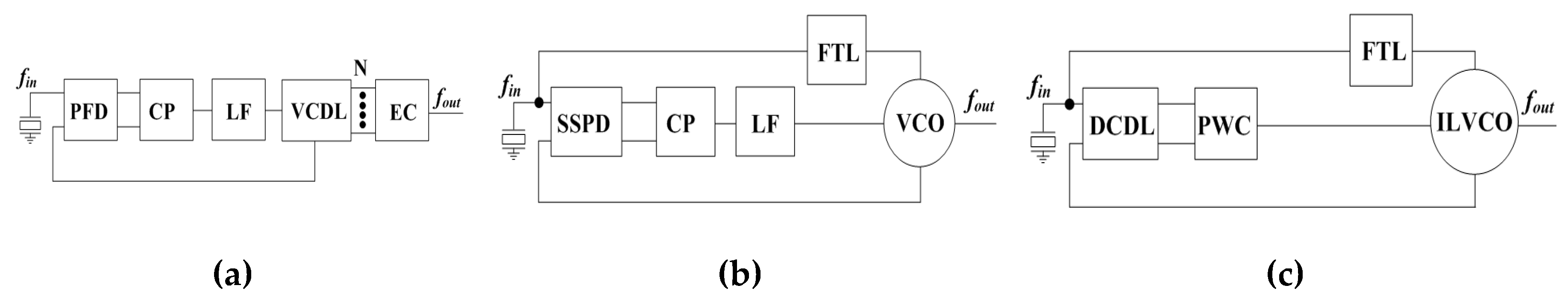
Figure 2.
The proposed synthesizer block diagram.
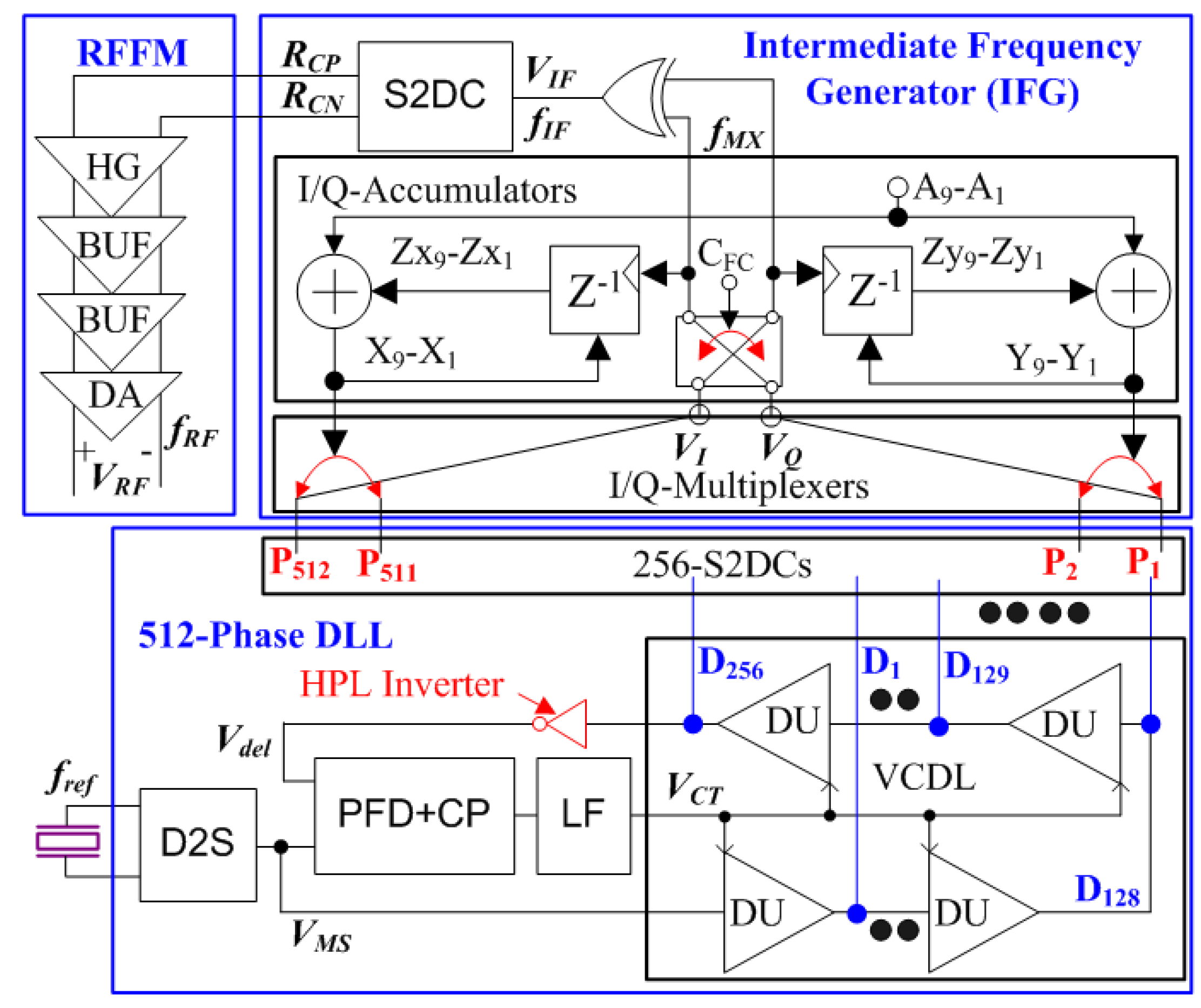
Figure 3.
256-S2DCs (a) Schematic. (b) Output waveforms.
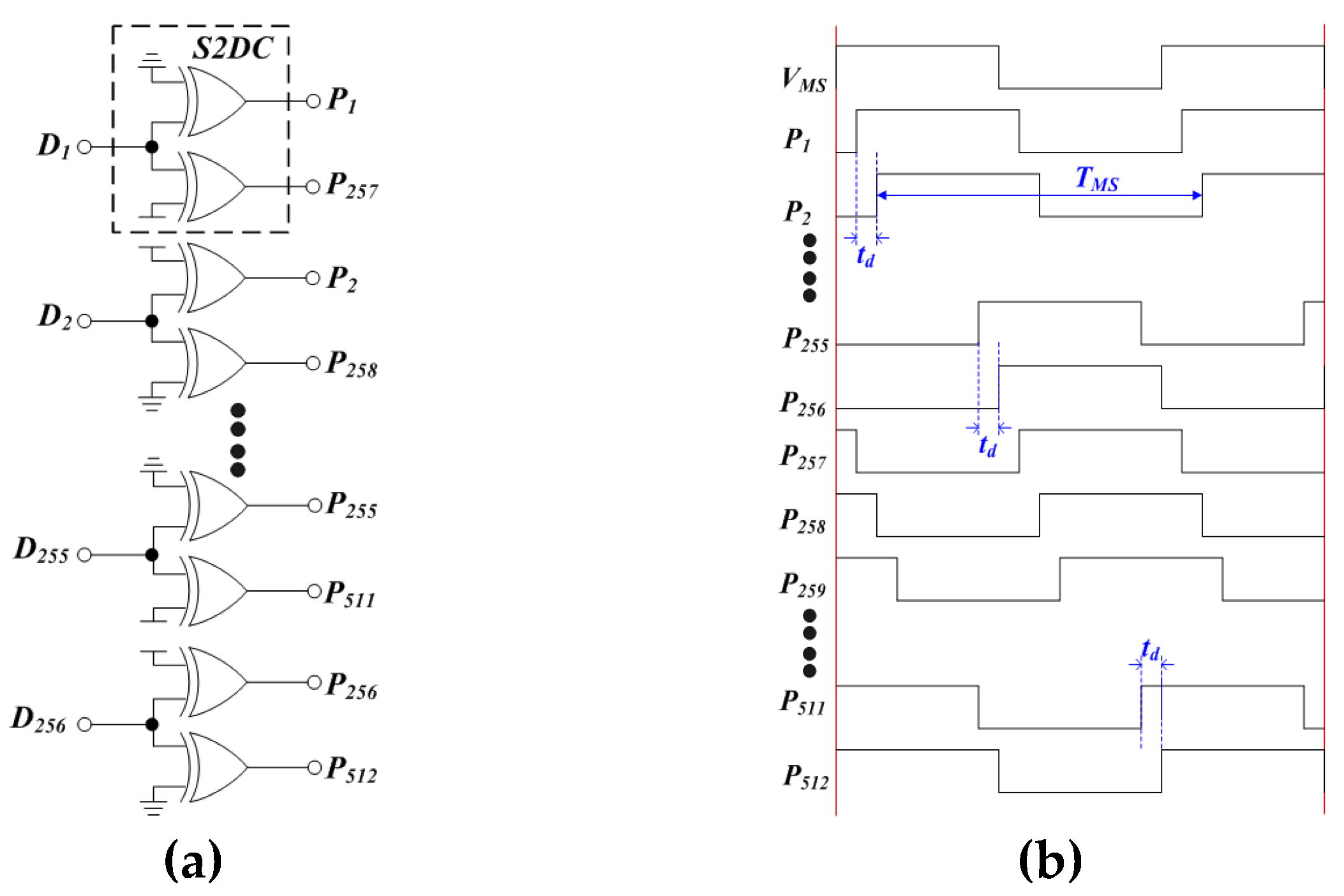
Figure 4.
(a) P1-P16, VQ and VI (18td period), and VQ (4td period) pulses. (b) VQ, VI, and VIF pulses when ACM = 2-6 and switching to phase lag. (c) VQ, VI, and VIF pulses when ACM = 1-5 and switching to phase lead.
Figure 4.
(a) P1-P16, VQ and VI (18td period), and VQ (4td period) pulses. (b) VQ, VI, and VIF pulses when ACM = 2-6 and switching to phase lag. (c) VQ, VI, and VIF pulses when ACM = 1-5 and switching to phase lead.
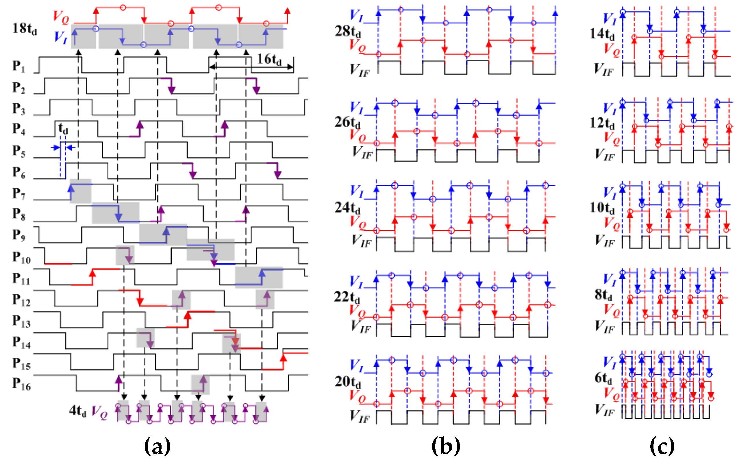
Figure 5.
VIF, VI, and VQ waveforms. (a) VIF is 50% duty cycle. (b) VIF are ±0.5td duty cycle offsets from the 50 % duty cycle.
Figure 5.
VIF, VI, and VQ waveforms. (a) VIF is 50% duty cycle. (b) VIF are ±0.5td duty cycle offsets from the 50 % duty cycle.
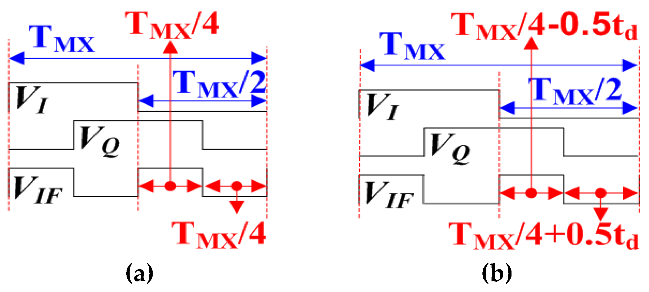
Figure 6.
Phase noise sources of the proposed synthesizer.
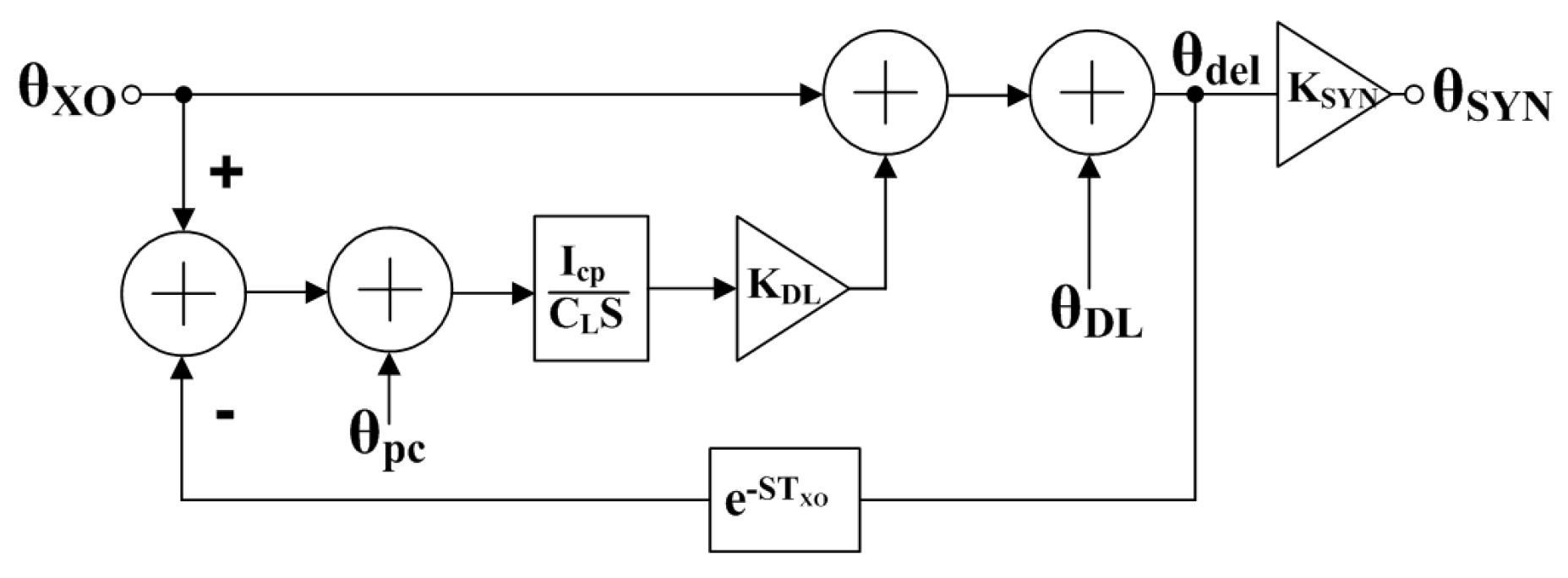
Figure 7.
Clock waveforms of (a) Ideal reference. (b) Jitter accumulated VCO.
Figure 8.
TSPC PFD schematic.
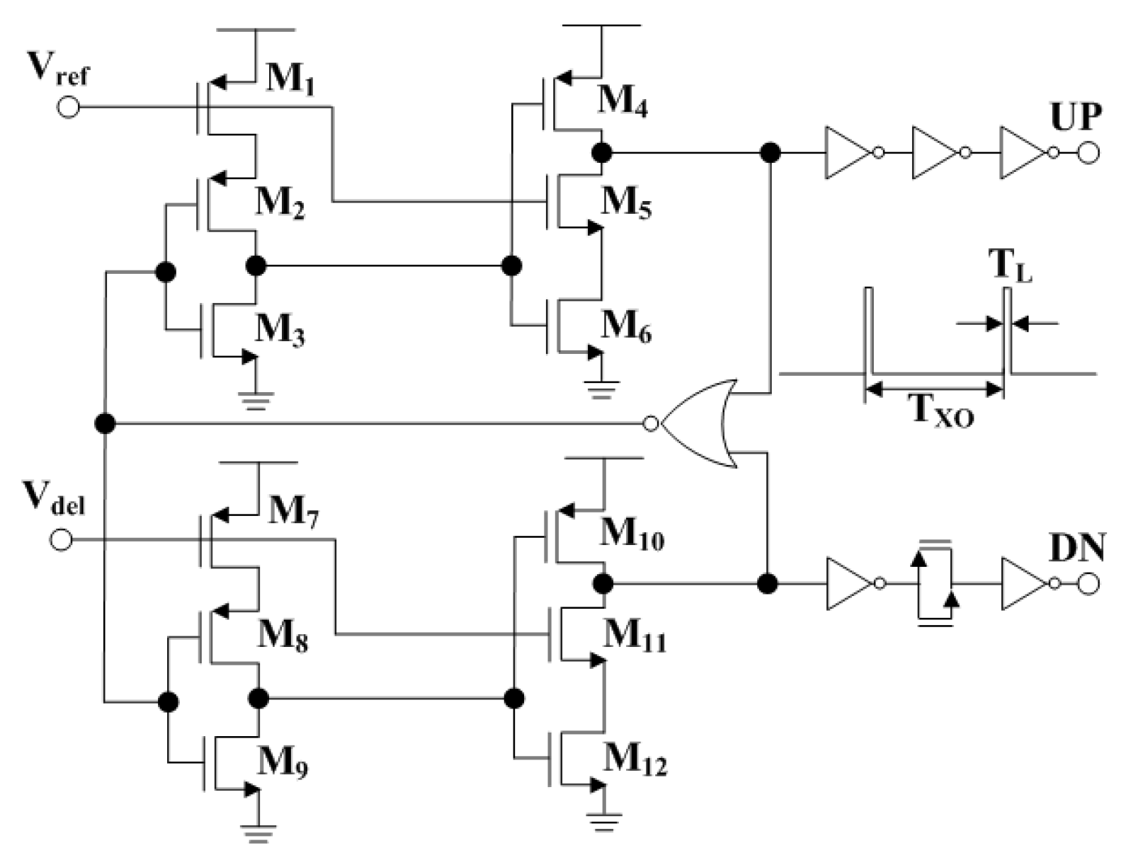
Figure 9.
Charge pump schematic.
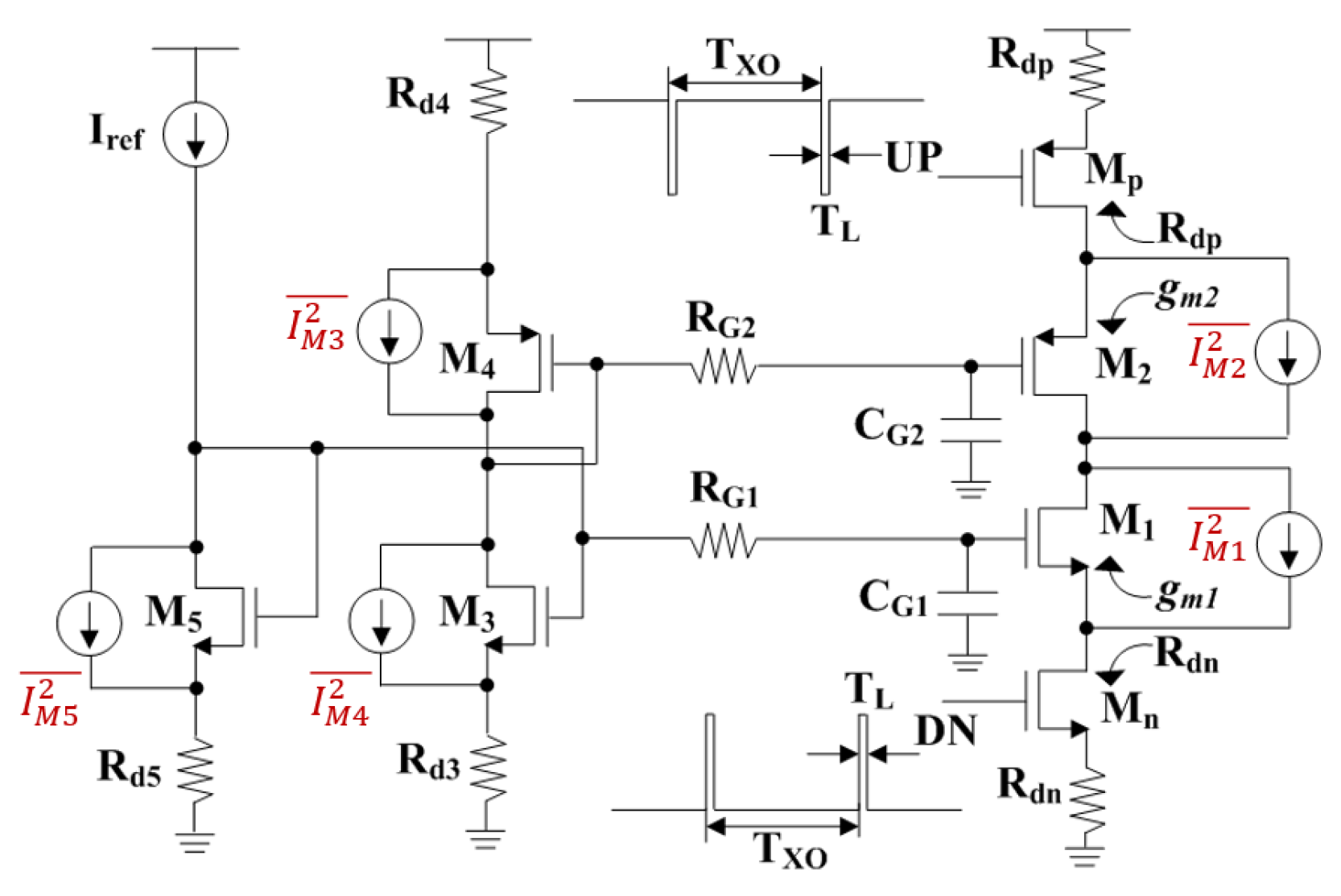
Figure 10.
The proposed PFD+CP PN simulations increase Rdn and Rdp as 62.5, 125, 250, 500, 1000, 2000, and 4000 Ω.
Figure 10.
The proposed PFD+CP PN simulations increase Rdn and Rdp as 62.5, 125, 250, 500, 1000, 2000, and 4000 Ω.
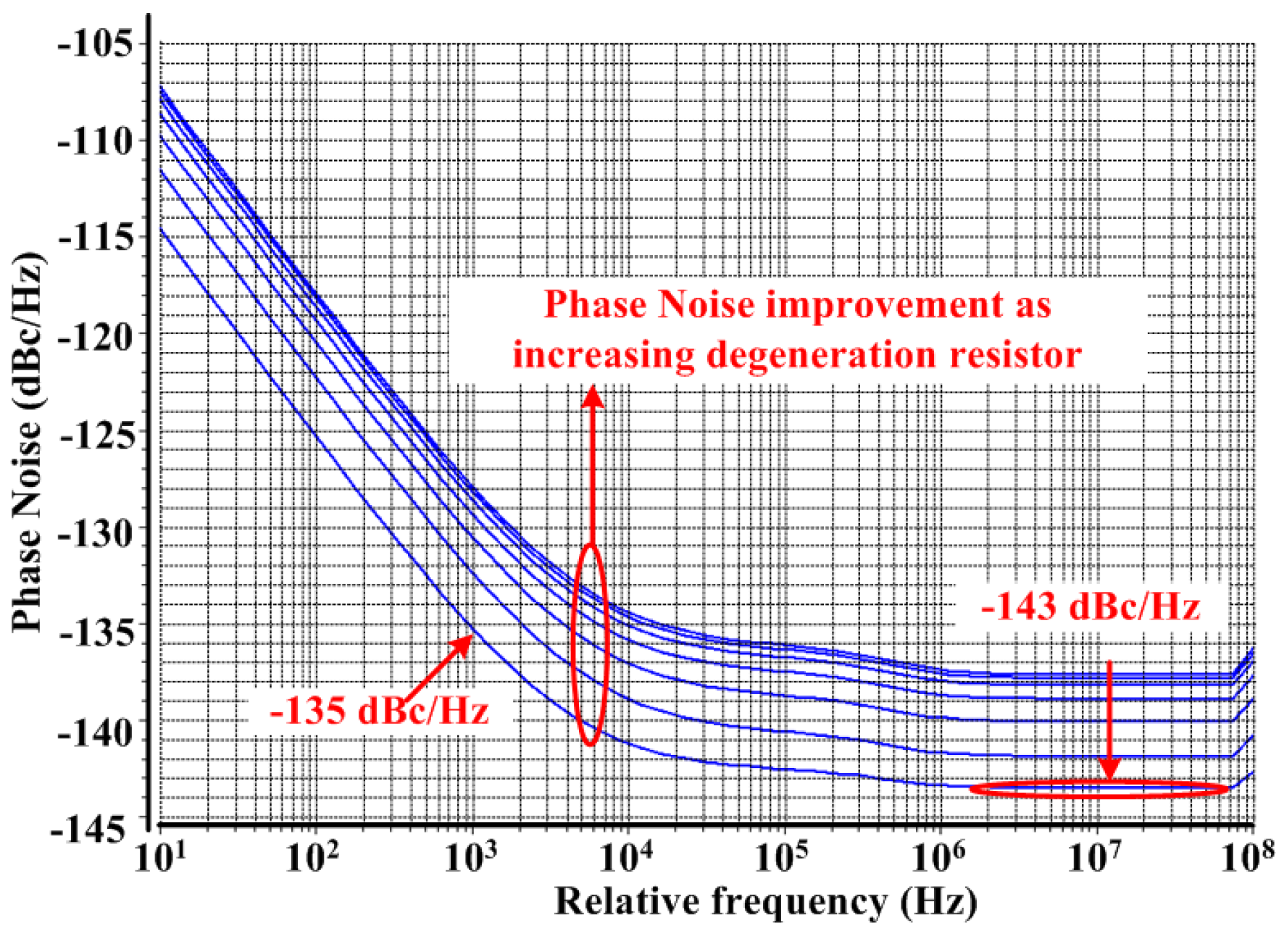
Figure 11.
Proposed schematic. (a) The first 255 DUs. (b) The last DU in the VCDL DU chain.
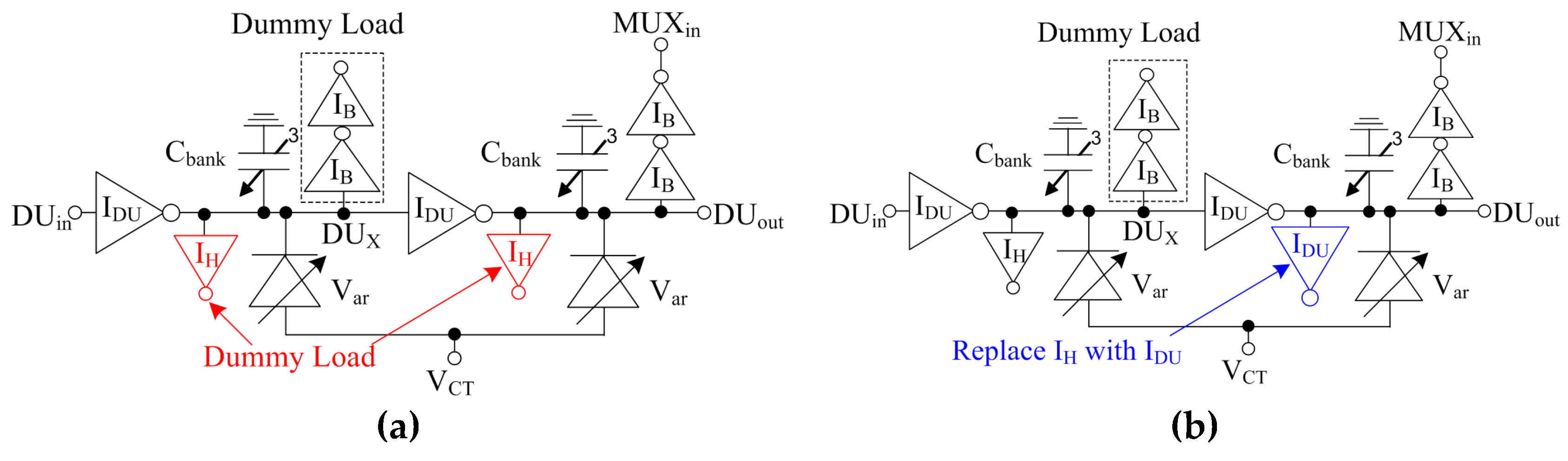
Figure 12.
DU SS/100ºC and FF/−20ºC simulation.
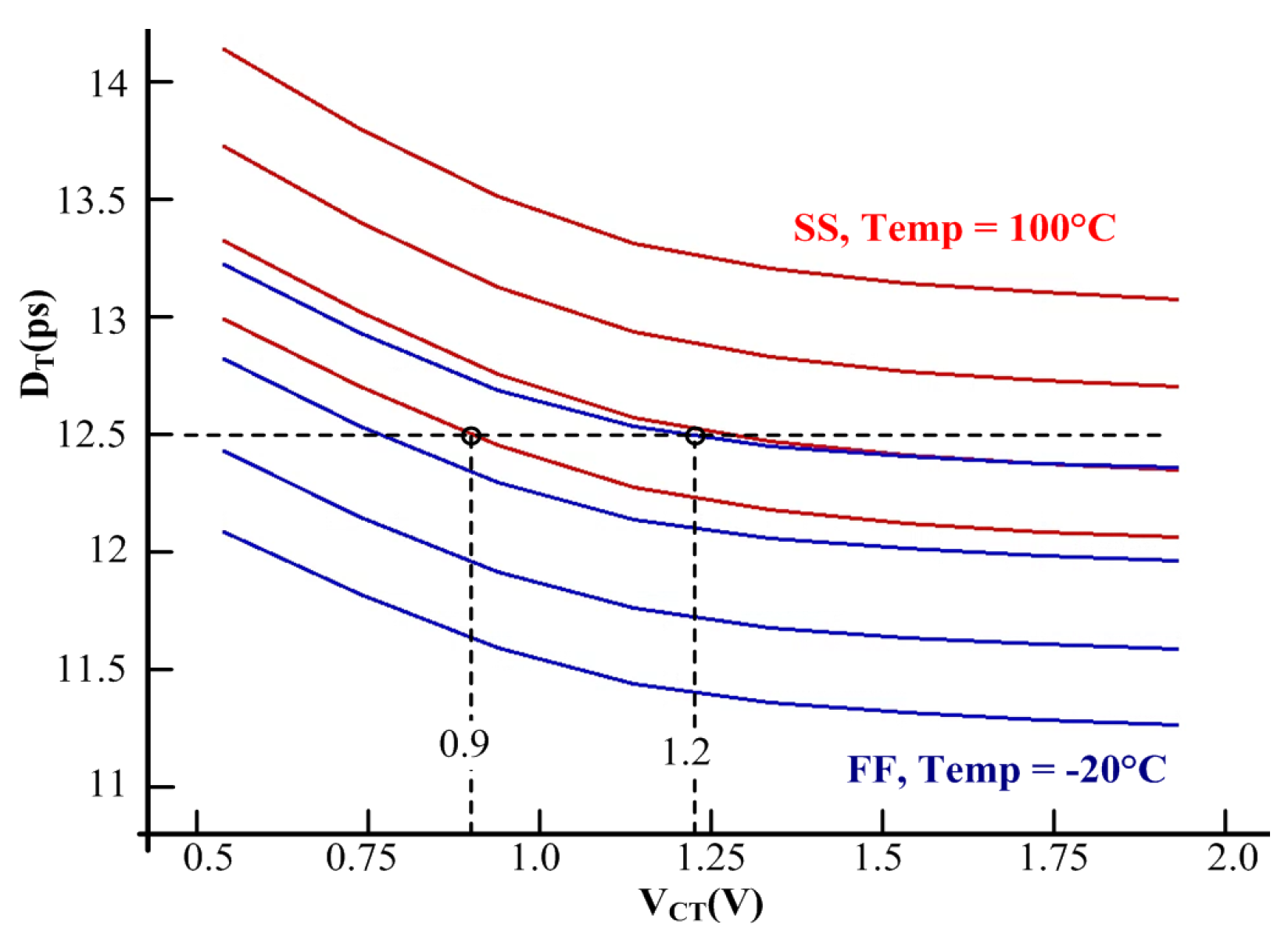
Figure 13.
PN simulations on DU16, DU32, DU48, DU64, and DU80 (blue curves) and estimated PN curve (red) on DU256.
Figure 13.
PN simulations on DU16, DU32, DU48, DU64, and DU80 (blue curves) and estimated PN curve (red) on DU256.
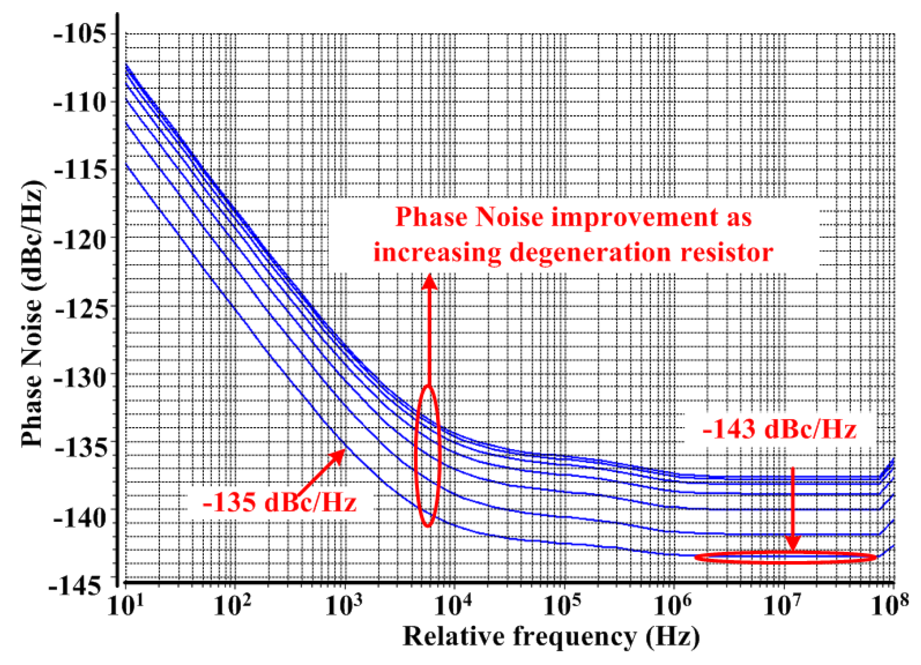
Figure 14.
(a) Jitter added P1-P16 waveforms. (b) Jitter added VPSP VPSN, and VXOR pulses for 14td (top) and 9td (bottom).
Figure 14.
(a) Jitter added P1-P16 waveforms. (b) Jitter added VPSP VPSN, and VXOR pulses for 14td (top) and 9td (bottom).
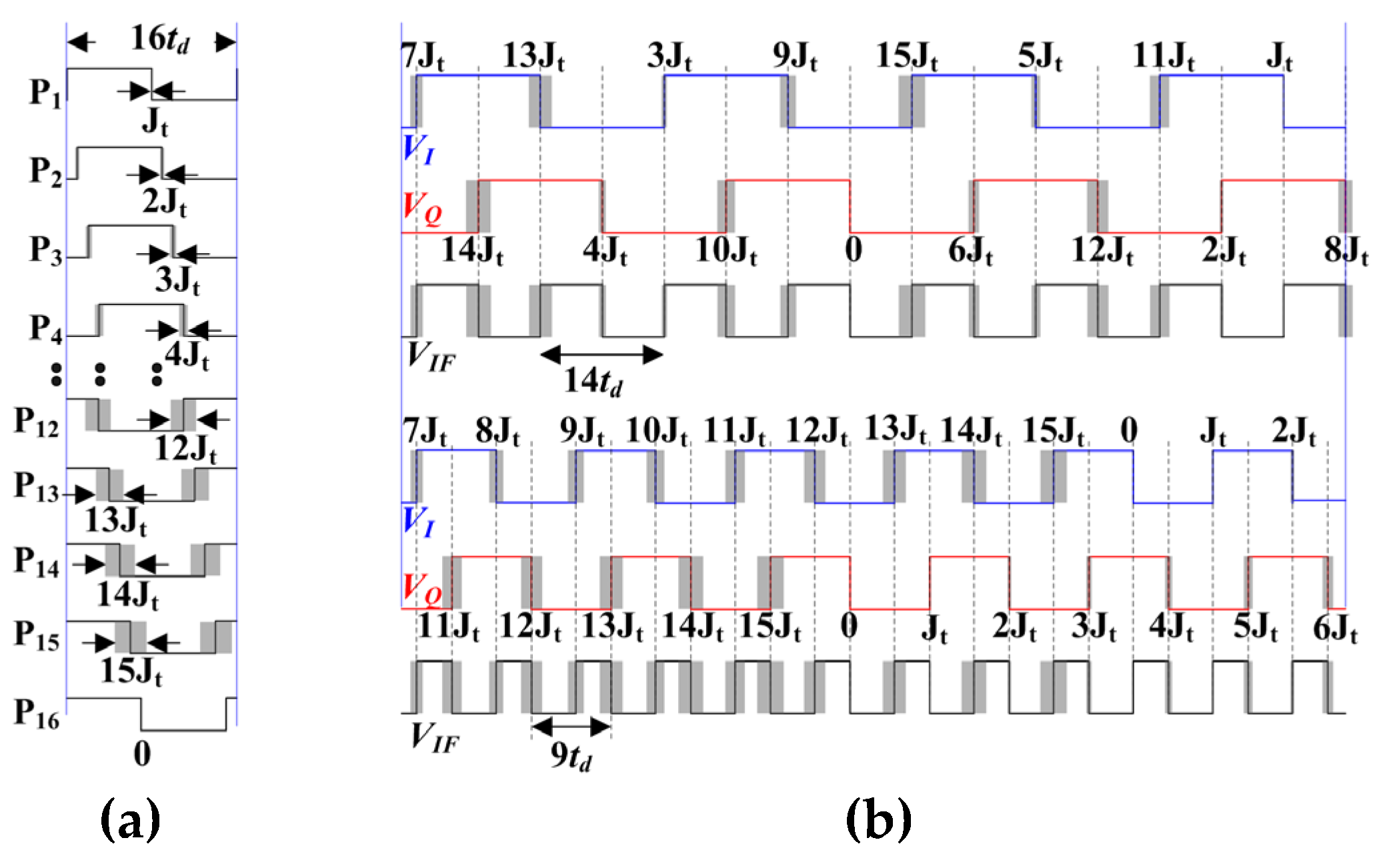
Figure 15.
Harmonic generator schematic.
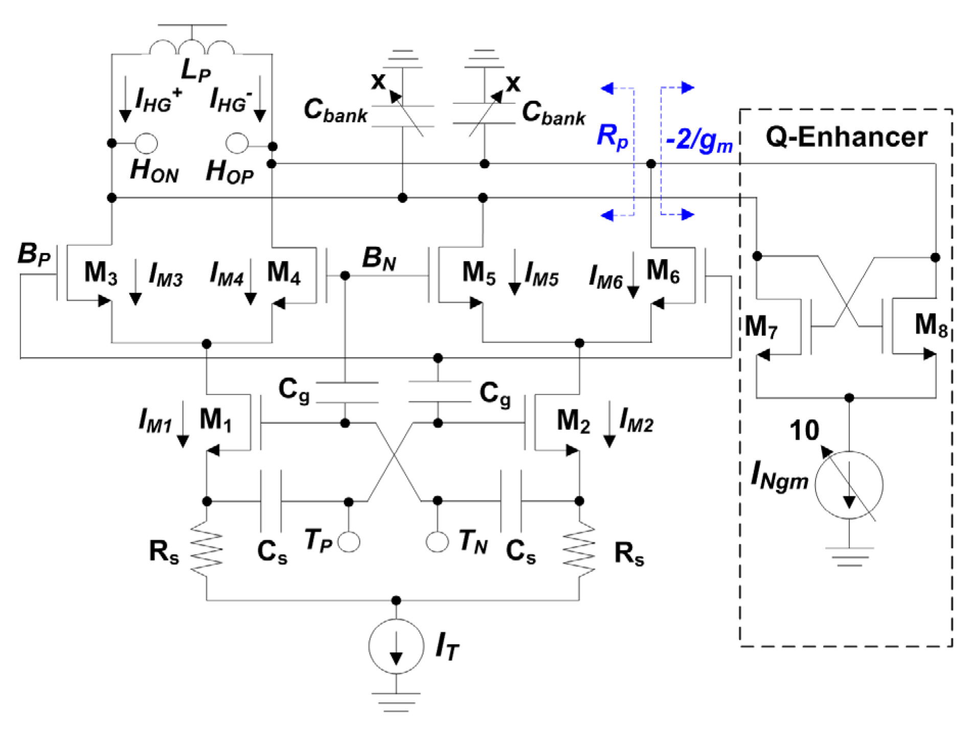
Figure 16.
Proposed HG ideal. (a) Internal voltage and current pulses. (b) Single and differential output current pulses.
Figure 16.
Proposed HG ideal. (a) Internal voltage and current pulses. (b) Single and differential output current pulses.
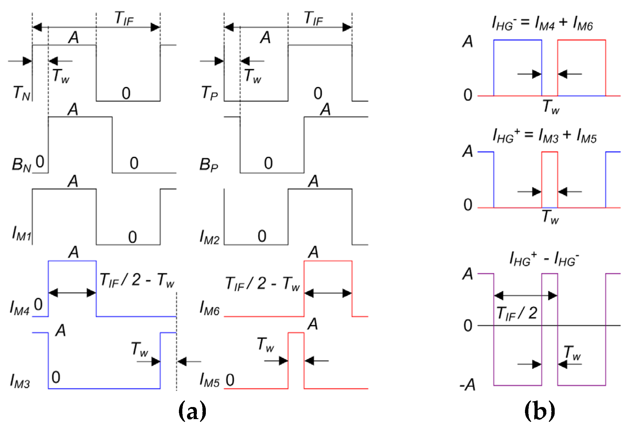
Figure 17.
Ideal (IHG+ − IHG-). (a) Pulse. (b) Spectrum. For ACM = 254, simulated (IHG+ − IHG-). (c) Pulse. (d) Spectrum. For ACM = 253, simulated (IHG+ − IHG-). (e) Pulse. (f) Spectrum.
Figure 17.
Ideal (IHG+ − IHG-). (a) Pulse. (b) Spectrum. For ACM = 254, simulated (IHG+ − IHG-). (c) Pulse. (d) Spectrum. For ACM = 253, simulated (IHG+ − IHG-). (e) Pulse. (f) Spectrum.
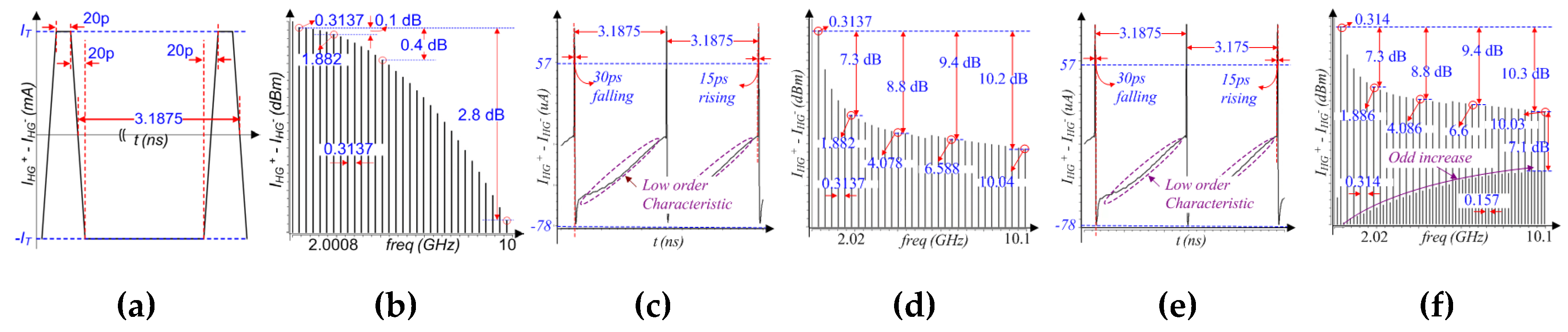
Figure 18.
(a) HG output LP-Cbank. (b) Equivalent parallel LP-Cbank. (b) When all M1–M10 are turned on. (c) When all M1-M10 are turned off.
Figure 18.
(a) HG output LP-Cbank. (b) Equivalent parallel LP-Cbank. (b) When all M1–M10 are turned on. (c) When all M1-M10 are turned off.
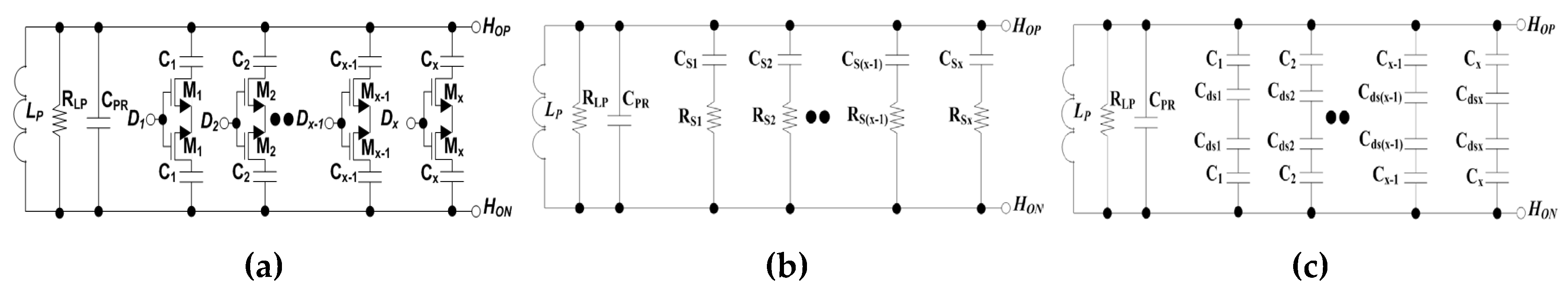
Figure 19.
HG differential output (HOP – HON) impedance simulations. (a) TT process at 25°C. (b) Zoomed simulations.
Figure 19.
HG differential output (HOP – HON) impedance simulations. (a) TT process at 25°C. (b) Zoomed simulations.
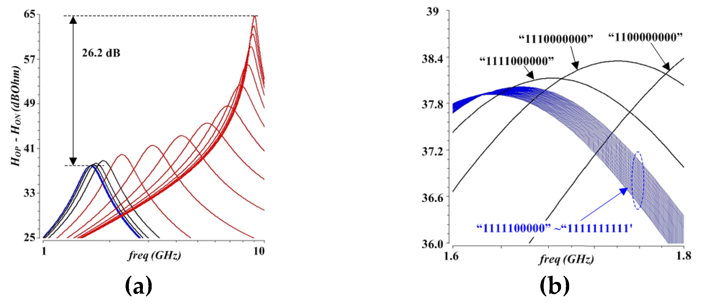
Figure 20.
HG differential output (HOP – HON) AC simulation for FF, TT, and SS processes. (a) Without negative-gm. (b) With negative-gm compensation.
Figure 20.
HG differential output (HOP – HON) AC simulation for FF, TT, and SS processes. (a) Without negative-gm. (b) With negative-gm compensation.
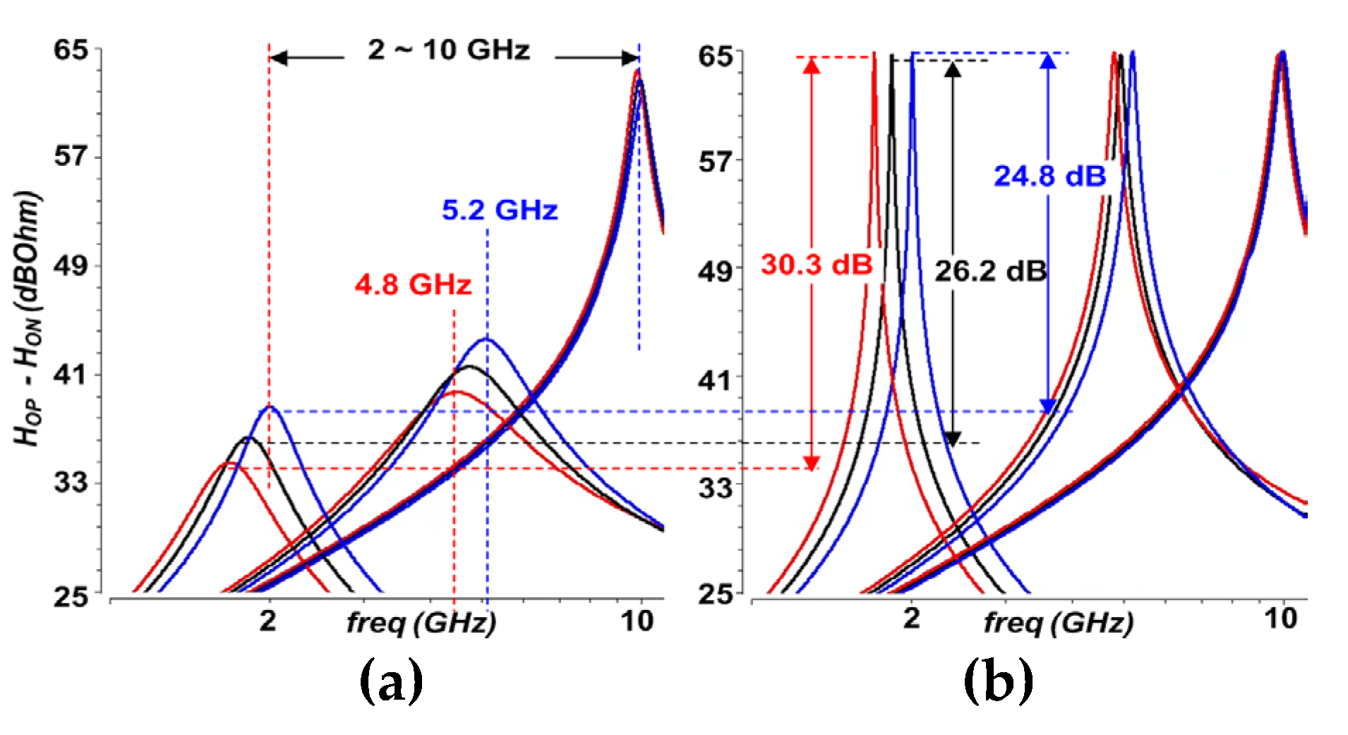
Figure 21.
Schematic of a buffer with an ACACL.
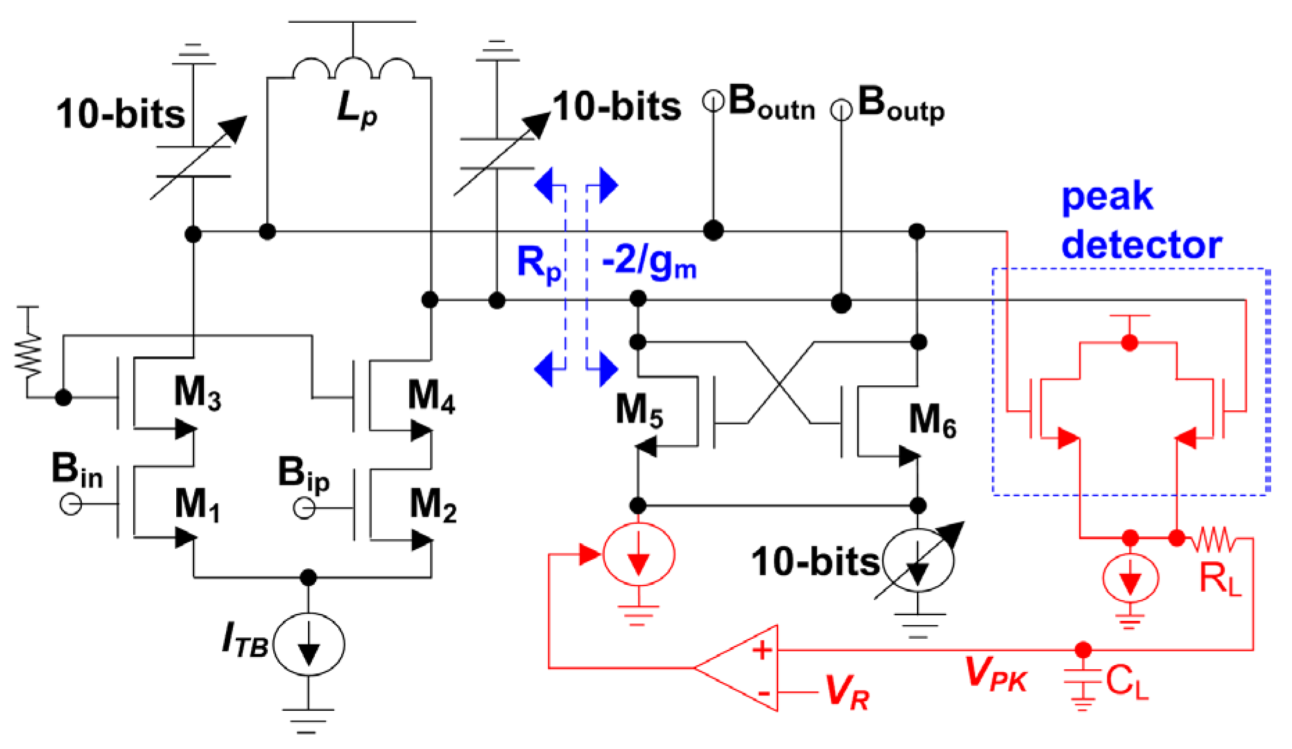
Figure 22.
For ACM = 253. (a) (IHG+ − IHG-) spectrum. (b) HG output spectrum. (c) First BUF output spectrum. (d) Second BUF output spectrum.
Figure 22.
For ACM = 253. (a) (IHG+ − IHG-) spectrum. (b) HG output spectrum. (c) First BUF output spectrum. (d) Second BUF output spectrum.
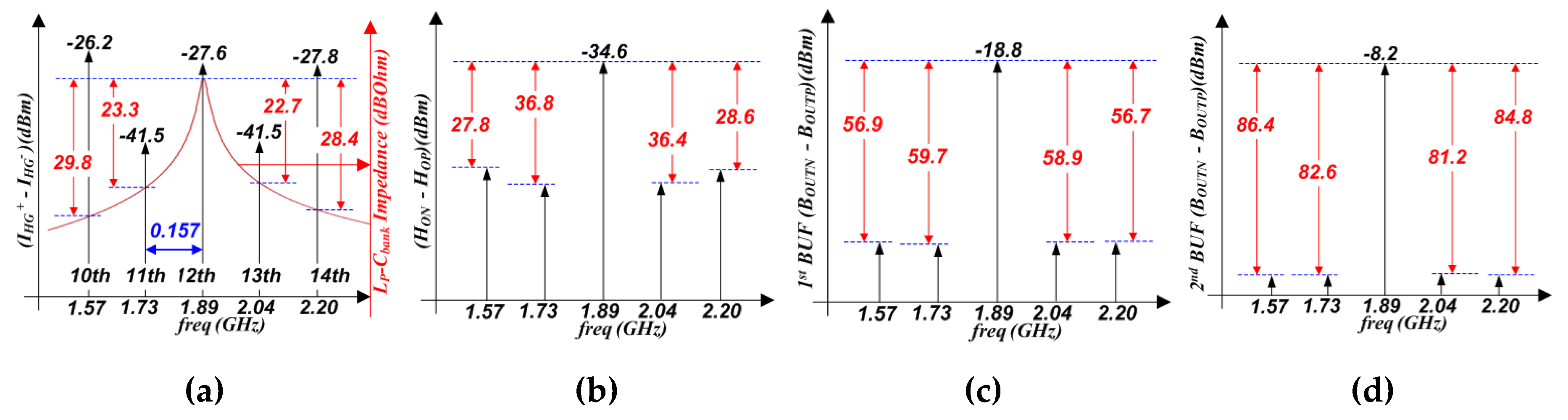
Figure 23.
The second BUF output spectrum. (a) ACM = 127. (b) ACM = 1.
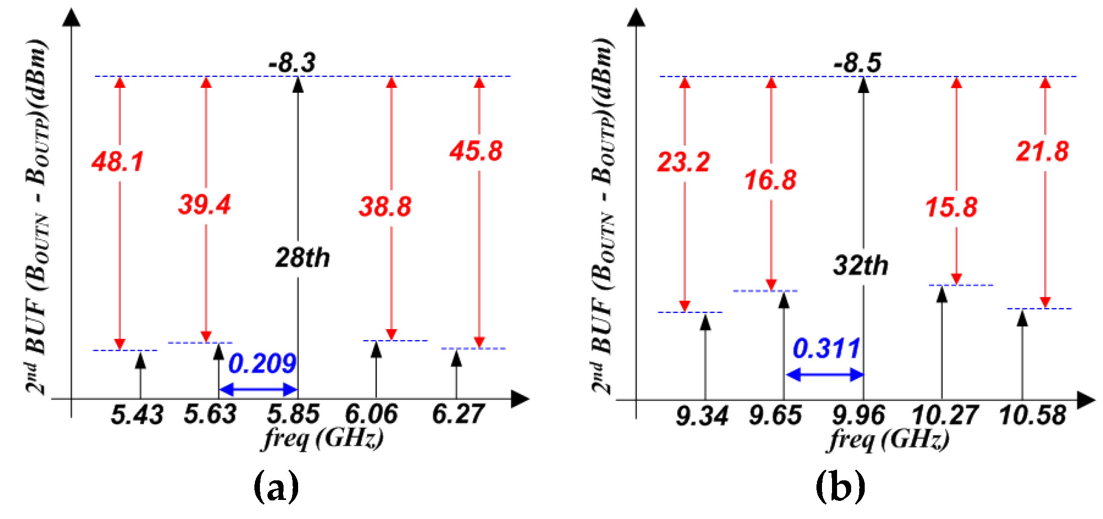
Figure 24.
Photograph of the proposed synthesizer.
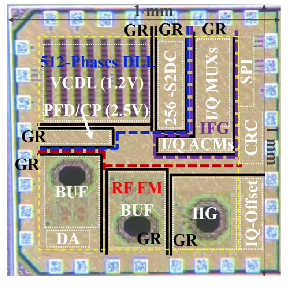
Figure 25.
Test environment block diagram.
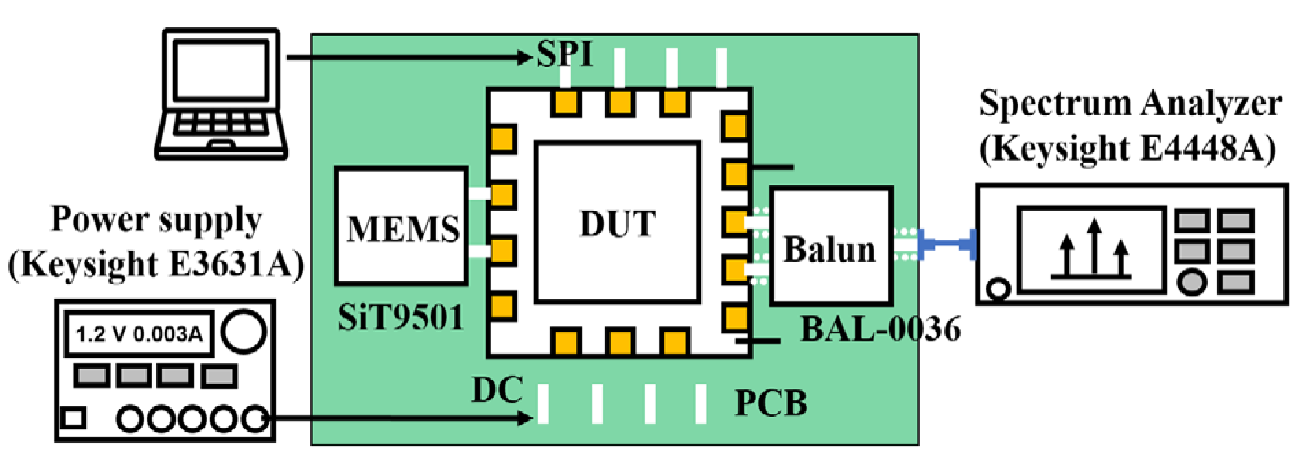
Figure 26.
Test environment block diagram.
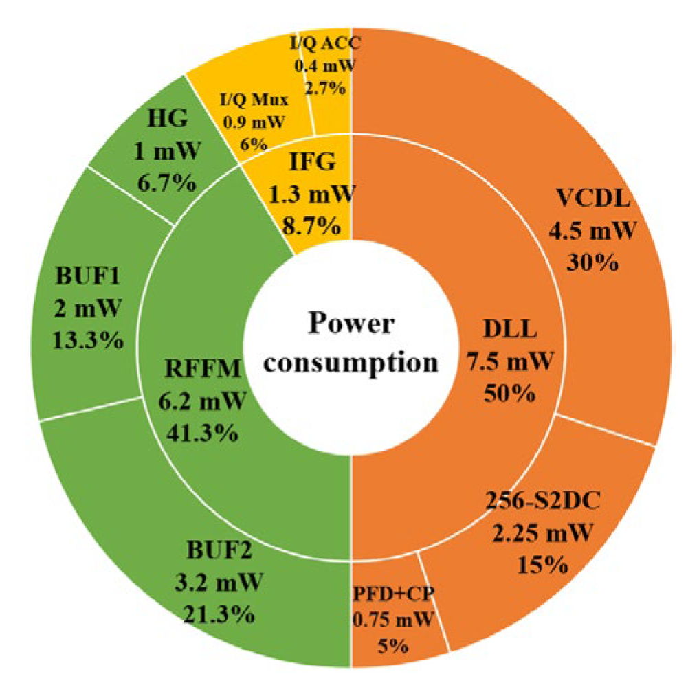
Figure 27.
Driver amplifier with external output matching.
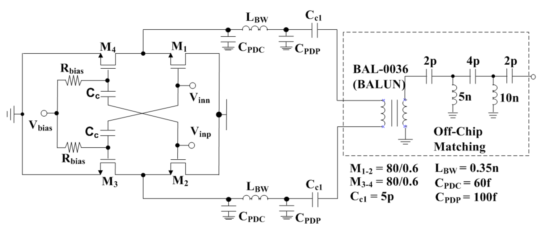
Figure 28.
DA. (a) OP1dB simulation. (b) S22 measurements of chip#1 ~ chip#5.
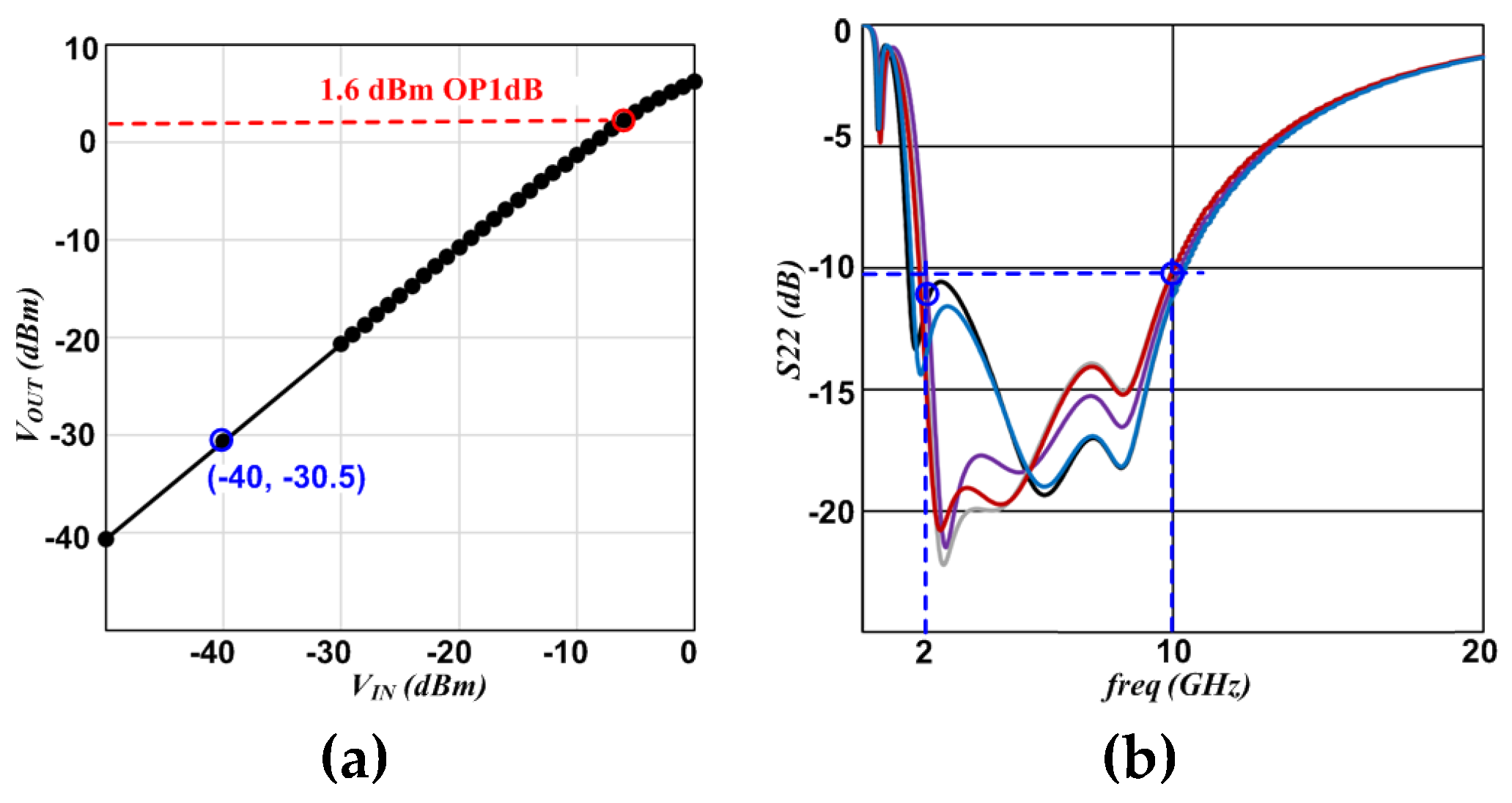
Figure 29.
Capacitor bank (Cbank) calibration block diagram.
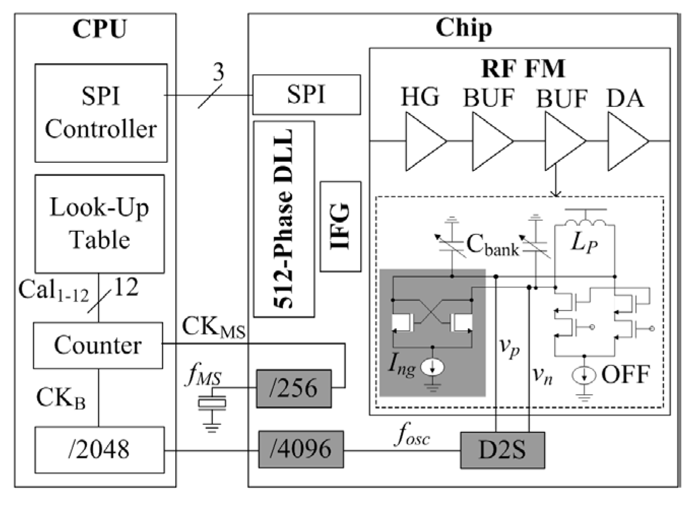
Figure 30.
Oscillating frequency calibration error.
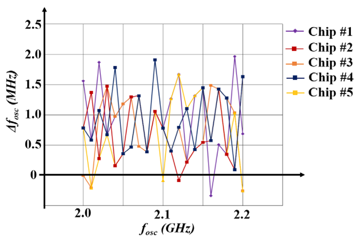
Figure 31.
The synthesizer output spectrum waveform. (a) ACM =1 and RFFMF =32. (b) ACM =2 and RFFMF =32. (c) ACM =127 and RFFMF =28. (d) ACM =128 and RFFMF =28. (e) ACM =253 and RFFMF =12. (f) ACM =254 and RFFMF =12.
Figure 31.
The synthesizer output spectrum waveform. (a) ACM =1 and RFFMF =32. (b) ACM =2 and RFFMF =32. (c) ACM =127 and RFFMF =28. (d) ACM =128 and RFFMF =28. (e) ACM =253 and RFFMF =12. (f) ACM =254 and RFFMF =12.
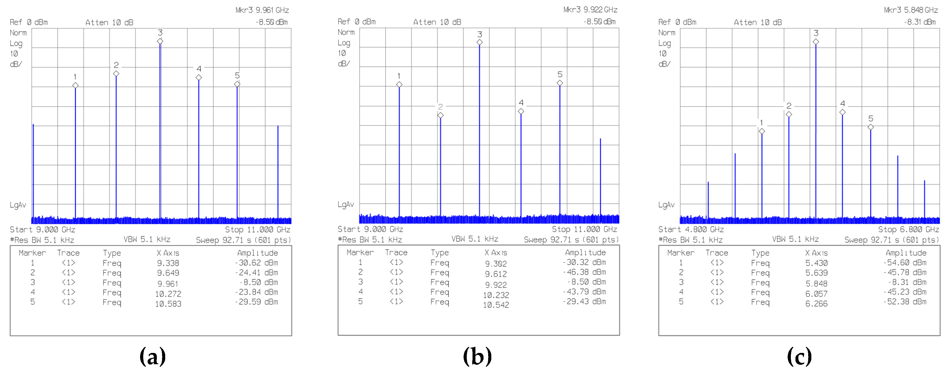
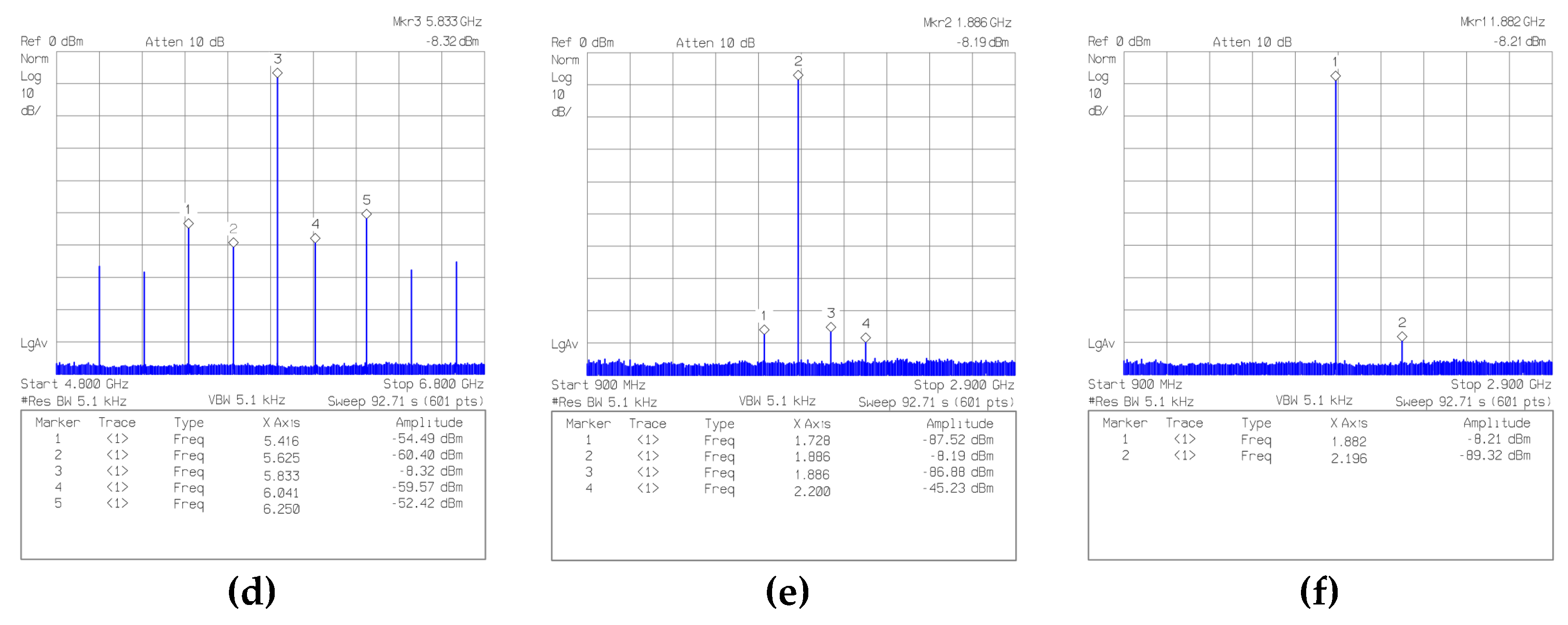
Figure 32.
The synthesizer output worst HRRs. (a) ACM = 1, 127, and 253. (b) ACM = 2, 128, and 254.
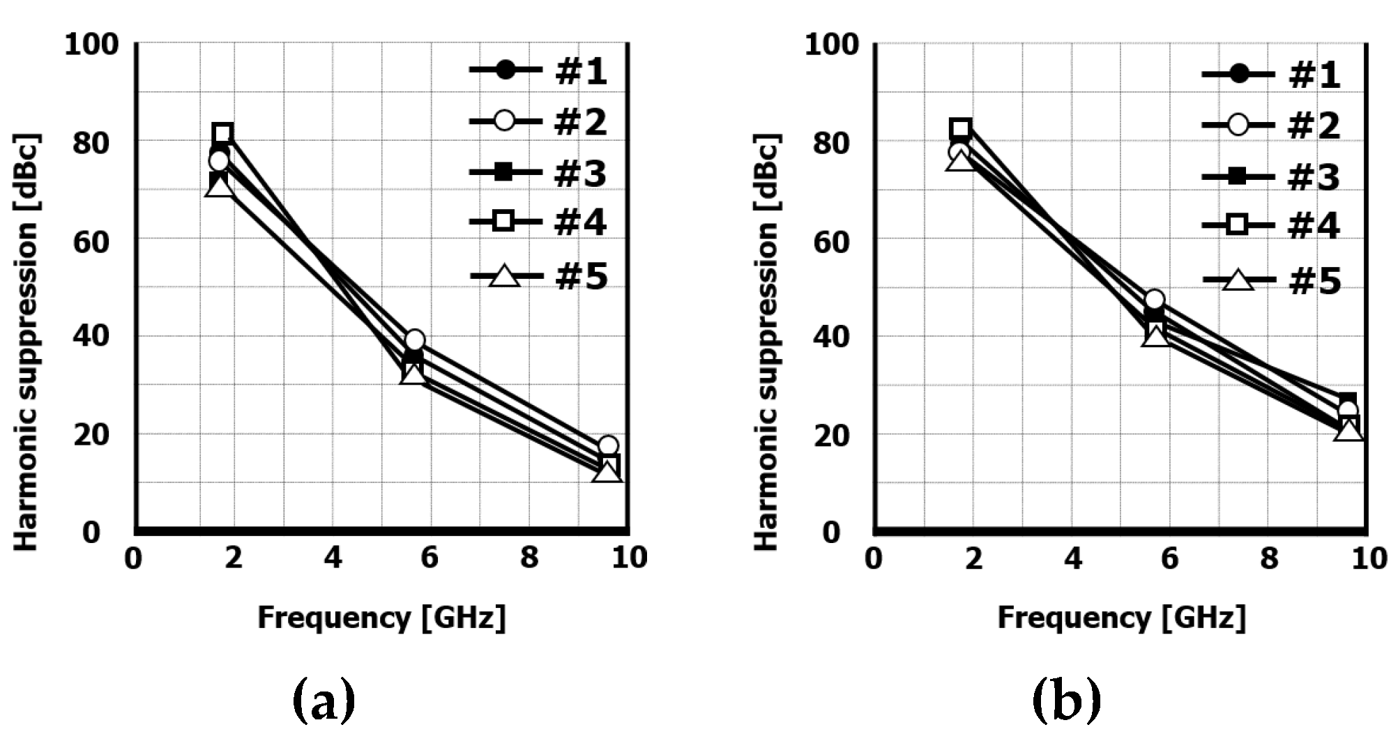
Figure 33.
The synthesizer PN curves of 1.89 and 9.96 GHz.
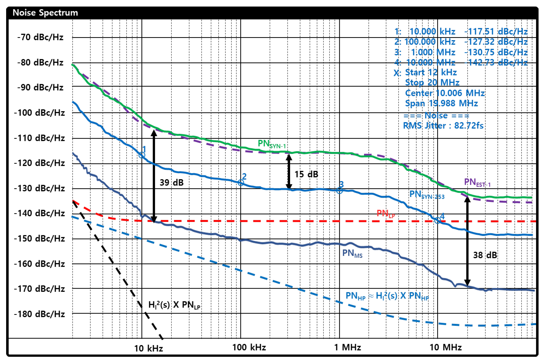

Table 1.
Counter Output.
|
Cbank D10-D1 |
Cal12-Cal1 Magnitude in decimal (Caldec) | ||||
| Chip#1 | Chip#2 | Chip#3 | Chip#4 | Chip#5 | |
| 1101010101 | 2561 | 2562 | 2561 | 2560 | 2560 |
| 1100101011 | 2499 | 2498 | 2499 | 2499 | 2499 |
| 1100000101 | 2400 | 2400 | 2439 | 2438 | 2439 |
| 1011100001 | 2382 | 2383 | 2382 | 2382 | 2383 |
| 1011000000 | 2328 | 2328 | 2328 | 2329 | 2327 |
Table 2.
RMS jitter measurement.
| Chip#1 | Chip#2 | Chip#3 | Chip#4 | Chip#5 | |
| RMS Jitter [fs] @ 1.89 [GHz] | 82.651 | 83.121 | 82.141 | 81.841 | 83.741 |
| 107.62 | 107.92 | 107.432 | 107.122 | 107.982 | |
| RMS Jitter [fs] @ 9.96 [GHz] | 82.721 | 83.541 | 82.341 | 82.211 | 84.131 |
| 107.572 | 107.832 | 107.482 | 107.242 | 108.052 |
1 Integrated from 12k to 20M. 2 Integrated from 1k to 100M.
Table 3.
Comparison with state-of-the-art synthesizer.
| Parameter | [19] | [20] | [21] | [22] | [23] | [28] | This work |
|---|---|---|---|---|---|---|---|
| Tech. | 65mm CMOS |
28mm CMOS |
28mm CMOS |
65mm CMOS |
65mm CMOS |
65mm CMOS |
65mm CMOS |
| fref [MHz] | 50.0 | 125.0 | 500.0 | 150.0 | 200.0 | 10 | 156.3 |
| fout [GHz] | 12–14.5 | 18.9–22.3 | 11.9–14.1 | 3–3.7 | 24–28.2 | 0.1–5 | 1.88–9.96 |
| Frequency Bandwidth [%] | 18.9 | 16.5 | 16.9 | 20.9 | 16.1 | 192.2 | 136.5 |
| rms jitter [fs] | 83.0 (1k-100M) |
71.8 (1k-100M) |
58.2 (1k-100M) |
135.0 (1k-100M) |
65.4 (10k-30M) |
9601 (10k-30M) |
107.6 (1k-100M) |
| Active Die area [mm2] | 0.2 | 0.5 | 0.2 | 0.4 | 0.5 | 1.44 | 0.6 |
| Power consumption [mW] | 7.7 | 36.0 | 18.0 | 9.5 | 14.5 | 21 | 17.0 |
| FoM12 | -252.8 | -247.3 | -252.1 | -247.6 | -252.1 | -227.1 | -246.9 |
| FoM23 | -265.5 | -259.5 | -264.4 | -260.8 | -264.1 | -250.0 | -268.25 |
1 Referred from phase noise plot. 2 3
Disclaimer/Publisher’s Note: The statements, opinions and data contained in all publications are solely those of the individual author(s) and contributor(s) and not of MDPI and/or the editor(s). MDPI and/or the editor(s) disclaim responsibility for any injury to people or property resulting from any ideas, methods, instructions or products referred to in the content. |
© 2024 by the authors. Licensee MDPI, Basel, Switzerland. This article is an open access article distributed under the terms and conditions of the Creative Commons Attribution (CC BY) license (http://creativecommons.org/licenses/by/4.0/).
Copyright: This open access article is published under a Creative Commons CC BY 4.0 license, which permit the free download, distribution, and reuse, provided that the author and preprint are cited in any reuse.


