
Submitted:
07 October 2024
Posted:
08 October 2024
You are already at the latest version
Abstract
This research aims to develop top-emission OLEDs (Organic Light light-emitting diodes) that exhibit enhanced electro-optical properties regarding color purity, luminance, efficiency, stability, and longer lifetime. To achieve this aim, we have used silicon wafer substrates with a thickness of 675 m. Top-emission OLED fabrication on silicon wafer substrates requires careful material selection and layer configuration. This device structure is described as follows: Silicon/Al (100 nm)/ HATCN (10 nm)/ Dic-TRZ: Ir(mppy)3 (40 nm)/ TPBi (30 nm)/ LiF 1.2 nm / Al 19.9 nm. LiF/Al combination is used as the semi-transparent cathode. Research on top-emission OLEDs has demonstrated the importance of silicon wafer substrates in enhancing electro-optical properties. The optical properties of top-emission OLEDs are significantly influenced by factors such as the semitransparent cathode layer's thickness and the anode layer's surface roughness. Study findings encompass the impact of microcavity on TEOLEDs, dopant concentration on device performance, and device thermal conductivity and lifetime. To create a highly efficient top-emission OLED on a silicon substrate, we meticulously fine-tuned parameters such as the thickness of the cathode Al layer (19.9 nm), the organic layer thickness (HIL - HATCN 10 nm, HTL - NPB 30 nm, ETL - TPBi 30 nm, EML - DIC–TRZ: Ir(mppy)3 40 nm), and the dopant concentration. Electro-optical performance has been significantly improved through optimization, especially in devices with high dopant concentrations. The 38% dopant concentration experiments resulted in a peak current density of 201.97 mA/cm2, a luminance of 4776 cd/m2, and an efficiency of 2.36 cd/A at 9 V. In addition, the high dopant concentration has resulted in a narrow spectral range, indicating a strong microcavity effect. Additionally, Si-TEOLEDs were tested for lifetime under these specific conditions, exhibiting a half-life of 420 hours.
Keywords:
Top-emission organic light-emitting diodes
; Electro-Optical Characteristics
; Silicon wafer
; Dopant concentration
; Lifetime
; Thermal conductivity
1. Introduction
One of the latest developments in OLED technology is the top-emitting OLED. Unlike conventional OLEDs, these OLEDs emit light from the top surface, providing various advantages. When using top-emitting OLEDs, displays can be created on opaque substrates, such as silicon wafers, which is impossible with bottom-emitting OLEDs. With this advancement, microelectronics and optoelectronics are now among the many applications of OLED technology. One of the main challenges of top emitters OLED is their transparent cathode. The use of conducting polymers, metal oxides, and metal grids has been studied to address this problem. Recently, new materials and fabrication techniques have been developed for top-emitting OLEDs. These advances allow top-emitting OLEDs to have more efficiency, stability, and color purity. For top-emitting OLEDs, researchers have focused on materials with high reflectivity at visible wavelengths and a high work function for efficient hole injection. These properties are crucial for achieving high luminance efficiency in top-emitting OLEDs [1,2,3].
Anodes on the bottom are crucial for achieving high efficiency. Two important properties are required for bottom anode materials: high reflectivity and the ability to inject holes into organic materials. Although aluminum (Al) and aluminum alloys have a high reflectivity over visible wavelengths, their work functions are relatively low. A metal with a high work function, such as platinum (Pt), nickel (Ni), molybdenum (Mo), etc., can efficiently inject holes into organic materials. Some materials, however, such as aluminum (Al), gold (Au), molybdenum (Mo), platinum (Pt), and vanadium (V), which have favorable electrical and optical properties, are not supported by the current complementary metal-oxide-semiconductor foundry [4,5]. In a general CMOS foundry, aluminum (Al), titanium (Ti), and tungsten (W) are some available materials for the anode in top-emitting OLEDs. Using these materials alone has limitations in terms of efficiency due to the low reflectivity of the anode. "Alternative approaches have been explored to utilize materials supported by general CMOS foundries, such as titanium nitride (TiN) and Al/TiN bilayer structures. TiN or an Al/TiN bilayer has been used as the anode in top-emitting OLEDs to enhance their performance while using materials compatible with general CMOS foundries." Ti and TiN anodes have low reflectivity, which limits the overall efficiency of OLEDs. [6,7,8,9,10]. Semitransparent cathodes commonly generate microcavity effects. Silver (Ag) can be used as a semitransparent cathode due to its low absorption rate. However, its high work function makes it difficult to use as a cathode. Furthermore, Al and Mg can be incorporated into TEOLEDs for superior electron injection. Indium Zinc Oxide (InZnO), Wo3, Ca, Sb, and Barium (BA) can also be used as cathode materials. It is possible to further enhance the microcavity effect by adding a capping layer (CPL). The cathode's and CPL's thickness play a significant role in the TEOLED microcavity effect [11,12].
Operating OLEDs generate thermal energy from electrical input, which increases with temperature. Sudden temperature spikes can cause organic layer crystallization, leading to failure. Changes in surface properties can degrade OLED performance. Using silicon substrates with high thermal conductivity can effectively dissipate heat [13,14,15].
Silicon wafers are a popular substrate material in the semiconductor industry due to their excellent mechanical, thermal, and electrical properties. They are highly stable and have low coefficients of thermal expansion, making them perfect for microfabrication. Researchers have conducted several studies on silicon-based OLED devices. H. Cho et al. demonstrated that the 2-stack tandem OLED exhibited 20,000 cd/m2 at 9 V, adaptable with CMOS circuit driving. According to the operating image of the fabricated microdisplay panel with white tandem OLED, the OLED structure was well-controlled and exhibited a white spectrum (0.26, 0.26) CIE coordinate and 28 cd/A current efficiency at 1,000 cd/m2. The efficient tandem OLED has been achieved by using ytterbium (Yb)/Ag bilayer materials as a cathode layer and a bilayer of aluminum (Al) and titanium nitride (TiN) as an anode layer [1]. Lee et al. developed the top-emitting WOLED on the silicon substrate, demonstrating a low driving voltage of 3.3 V while producing 4,200 cd/m2 of white light (0.34, 0.36), the CIE color coordinates for the emitted light. Furthermore, the device can emit cool white light with a maximum luminance of 170,000 cd/m2 [2]. Y. Motoyama et al. developed a 0.23-inch M-OLED display with a luminance of 5000 cd/m2 and a high resolution of nHD by utilizing a microlens array, an InZnO cathode and optimizing the spectral transmittance of the color filter [3]. P. Ghosh et al. researched high-resolution OLED-on-silicon microdisplays with small subpixel dimensions (2-5 microns). They used high-Tg materials and thin films for hermetic sealing. After testing for over 2600 hours, no significant reduction in luminance was observed [16]. According to Zhao et al. the efficiency of top-emission OLEDs can be significantly improved by using a metal Sm-modified n-Si cathode and a V2O5/Au anode with surface modification through antimony (sb) doping [17]. H. Lee et al. investigated the optical reflectivity, surface roughness, and sheet resistance of different anode layers (Al/TiN, Ti, and W) on silicon substrates commonly used in CMOS foundries. They also compared the current density-voltage characteristics of hole-only devices (HODs) with these metal layers as anodes [4]. K. Bouzid et al. optimized the trilayer cathode structure to improve the light out-coupling efficiency of OLEDs. They compared a WO3/Ag/WO3 cathode to a Ca/Ag cathode in a reference device. Simulation calculations predicted an approximately 40% increase in luminance, later confirmed experimentally [18]. Han et al. developed the TOLED by adding a 3 nm thick Cr layer as a hole-injection layer in an AlNd alloy anode. This configuration improved current efficiency to 6.3 cd/A, attributed to the high reflectivity of the anode [5]. Chung et al. studied how the thermal conductivity of substrates affects heat dissipation and the lifespan of OLEDs. Specifically, the researchers examined the impact of highly thermally conductive substrates like silicon wafers on OLED performance [13]. According to Park et al. they investigated the characteristics of reflective aluminum (Al) anodes for OLED devices. They constructed a high-efficiency green top-emitting OLED by improving the hole-injection characteristics of the Al anode. The OLED device with an Al anode achieved an efficiency of 35 cd/A at a brightness level of 1000 nit [10]. Xie et al. conducted a study that successfully lowered the operating voltage of TEOLEDs, which emit high brightness, to below 5 V. This enables foundries to utilize low-cost CMOS substrates without providing high-voltage options. When combined with C545T fluorescent dye, the p-doped TEOLED can achieve a high brightness of 10,000 cd/m2 at 4.9 V, a desirable low operating voltage for lighting and displays [19].
1.1. Microcavity Phenomenon in (Top- Emission OLED)
Reflections in TE-OLED electrodes cause more complex interferences than in BE-OLED electrodes. In addition to the two-beam interference, there is a multi-resonance interference between both electrodes. A TEOLED resembles a Fabry-Perot resonator since both contain parallel mirrors (corresponding to reflective electrodes).
The output spectral intensity of a TEOLED is determined by two main optical effects: two-beam interference and Fabry-Perot interferences. These effects are collectively referred to as the 'micro-cavity effect.' To achieve constructive interference and enhance emission at specific wavelengths, the device thickness is adjusted based on the resonance wavelengths of blue (460 nm), green (530 nm), and red (610 nm) colors. The complex and thick device structure must be carefully designed in advance to fabricate the TE-OLED successfully. The device can be treated as a Fabry-Perot resonator to predict the output spectral intensity.
Microcavities result from multiple reflections between a reflective anode and a semitransparent cathode. OLED devices with reflective anodes and semitransparent cathodes, which employ reflective cathodes, experience micro cavitation. For active matrix displays, understanding and studying micro cavitation is crucial. As a result of microcavity structure changing emission spectra (narrows the broad emission spectra) and emission profiles, it can be used to enhance the performance of OLED devices. The following equation describes the microcavity condition [11,12,20].
2. Experiment Process
Top-emission organic light-emitting diodes (TE-OLED) 10 x 5 mm were successfully fabricated on a silicon substrate. The device pattern and material deposition are shown in Figure 1 (a) and (b).
The Si substrate (purchased from Summit-Tech Resource Corp, Taiwan) was soaked in acetone, isopropanol, and de-ionized water for 30 minutes each using an ultrasonic cleaner. Afterward, the substrate was dried with a nitrogen gun (N2) and then placed under a UV light for 20 minutes. Following this, organic and metallic layers was deposited using a thermal vacuum evaporation system at a vacuum pressure of 8.0 x 10⁻⁶ torr. Initially, a reflective anode of Al (100 nm) was deposited at a rate of 4.5-5 Å/s. Once the anode layer was deposited, the substrate was shifted to the organic evaporator. Dipyrazino [2,3-f:2',3'-h]quinoxaline-2,3,6,7,10,11-hexacarbonitrile (HATCN) is employed as the hole-injection layer (HIL), N,N′-Di(1-naphthyl)-N,N′-diphenyl-(1,1′-biphenyl)-4,4′-diamine (NPB) as the hole transport layer (HTL), 2,4-diphenyl-6-bis(12-phenylindolo) [2,3-a] carbazole-11-yl)-1,3,5-triazine (DIC-TRZ) Thermally Activated Delayed Fluorescence (TADF) as host emitting material, Tris[2-(p-tolyl)pyridine]iridium(III), Ir(mppy)3 as dopant emitting material, and 2,2',2"-(1,3,5-Benzinetriyl)-tris(1-phenyl-1-H-benzimidazole) (TPBi) as electron transport layer (ETL). The semi-transparent cathode is composed of LiF/Al. The top-emission OLED on the Silicon substrate, energy band diagram, and device structure are shown in Figure 2 (a) and (b).
The Si-TEOLEDs are protected from external factors like moisture and oxygen through encapsulation, which helps to maintain the performance of the OLED device. The silicon substrates are encapsulated with glass covers, which are carefully aligned and positioned on top of the silicon substrate. Once the cover glass is correctly aligned, pressure is applied to ensure close contact between the glass, glue, and silicon substrate. The UV glue is exposed to 90 mW UV light for 300 seconds to achieve strong adhesion, and the Si-TEOLED encapsulation flow process is shown in Figure 3.
After encapsulating the Si TEOLED device, we used the Keithley 2400 to bias the green OLED. Then, we measured its luminance and spectra using the Spectra Scan PR 650 Spectral Colorimeter. Following the measurement of the I-V-L data, the TEOLED has undergone a lifetime measurement to monitor its long-term durability and reliability. The measurement system is illustrated in the Figure 4.
3. Results and Discussion of Silicon-Based TE-OLED Device
The silicon substrate is used in TE-OLEDs, offering advantages such as integration with CMOS technology, greater luminance, current density, efficiency, and longer device lifespan. These TE-OLEDs also possess the inherent benefits of OLEDs, including high-contrast displays, wide viewing angles, and excellent color reproduction.
As part of this study, we optimize the thickness of a semi-transparent cathode layer, the organic layer, and the surface roughness of anode layer, which affects the TE-OLED's optical properties and microcavity effect on TEOLED. The optimized device structure is as follows: Si/Al (100 nm)/ HATCN (10 nm)/ NPB (30 nm)/ DIC-TRZ: Ir(mppy)3 (40 nm)/ TPBi (30 nm)/ LiF (1.2 nm)/ Al (19.9 nm).
3.1. Semitransparent Cathode Layer
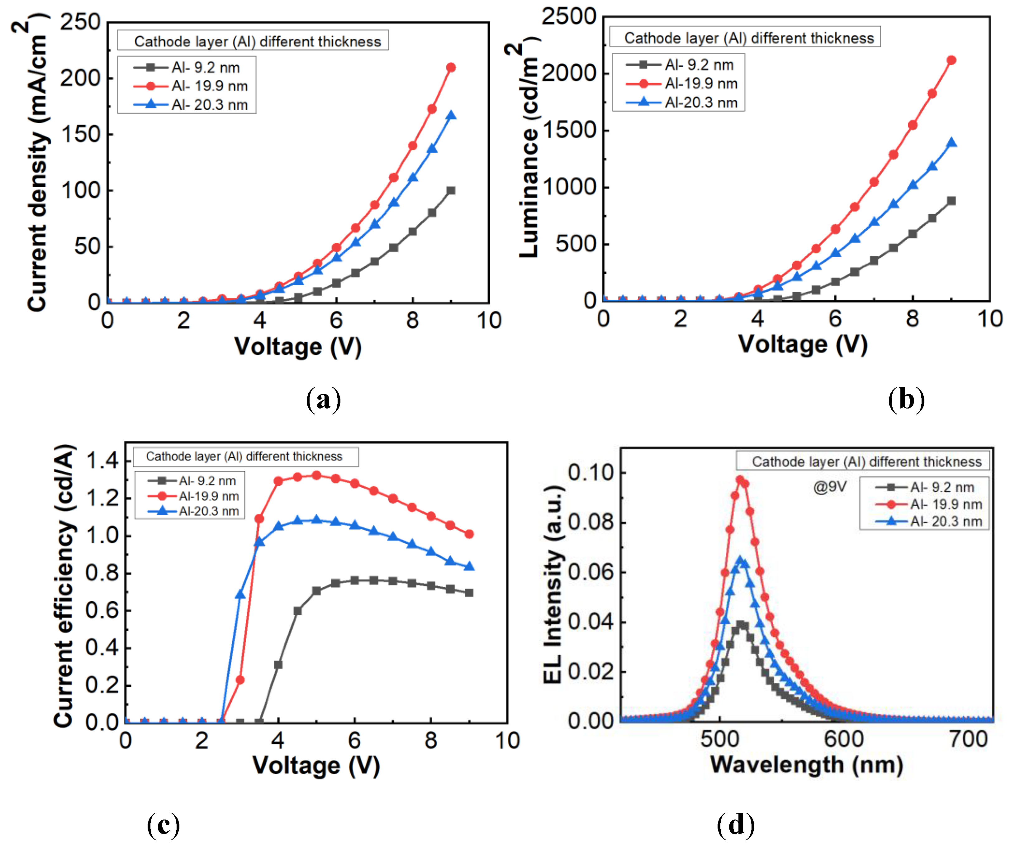
For optimal performance, microcavity-based TEOLEDs require a cathode that is semitransparent, highly reflective, and low-absorbent. It is crucial for the cathode to efficiently inject electrons into its adjacent ETL. An experiment was conducted to find the optimal thickness for semitransparent cathode layers on a glass substrate. The experiment measured transmittance (T), reflection (R), and absorption (A) within the visible wavelength range of 420-720 nm and calculated the average values for T, R, and A. The 20.3 nm Al layer demonstrates a low transmittance of 5%, a high reflectance of 83%, and a high absorption of 1.3 a.u., which may limit the OLED's light-emitting capabilities. On the other hand, the 19.9 nm Al layer shows an average transmittance of 12%, a reflectance of 80%, and an absorption of 0.9 a.u., making it a suitable thickness for the semitransparent cathode layer. The Al layer, measuring 9.2 nm in thickness, demonstrates a relatively high transmittance of 16%, along with a low reflectance of 78% and low absorption of 0.8. However, due to its low reflectance, the 9.2 nm thickness may not be suitable for a semitransparent cathode. For further details, please refer to Table 1 and Figure 5, which presents the transmittance (T), reflectance (R), and absorption (A) values for a range of Al thicknesses.
Experimental approaches have also been conducted based on the T, R, and A values for various cathode layer thicknesses in order to determine the optimal thickness. An appropriate thickness is determined by comparing the current density–voltage (J–V), luminance–voltage (L–V), yield voltage (Y-V), and EL spectrum characteristics results, as shown in Figure 7 (a), (b), (c), and (d). The TEOLED device showed low electro-optical properties with cathode layer thicknesses of 9.2 nm and 20.3 nm. However, the device performed better with a 19.9 nm cathode layer, demonstrating a higher current density of 209.89 (mA/cm2), luminance of 2120 (cd/m2), current efficiency of 1.01 (cd/A) at 9 V. Therefore, the 19.9 nm (Al) cathode layer thickness was selected for further study.
Figure 6.
Experimental Emission photo of: (a) Al-9.2 nm; (b) Al-19.9 nm; (c) Al-20 nm. .
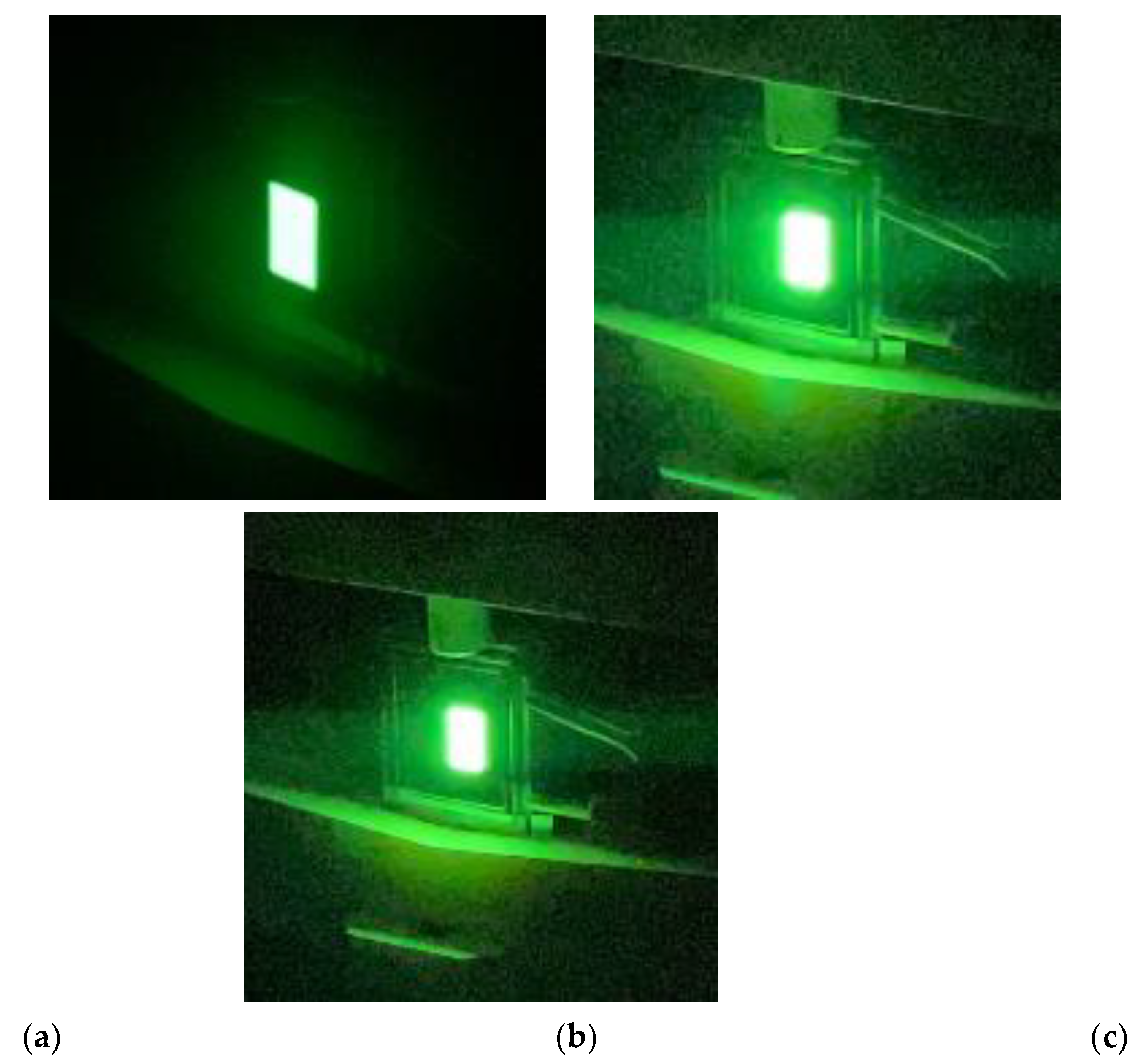
Figure 7.
Comparisons of (a) J–V; (b) L–V; (c) Y-V; and (d) EL spectrum of Si-TEOLED with different Al thicknesses for the cathode layer.
Figure 7.
Comparisons of (a) J–V; (b) L–V; (c) Y-V; and (d) EL spectrum of Si-TEOLED with different Al thicknesses for the cathode layer.
3.2. Anode Layer Surface Roughness
Optimizing the roughness of the anode layer is crucial because it can impact various properties of OLED devices, such as light extraction efficiency, electrical conductivity, and lifetime. For an Al thickness of 100 nm, the average roughness (Ra) is 2.82 nm, the root mean square roughness (Rq) is 4.09 nm, and the maximum roughness (Rmax) is 58.5 nm. Figure 8 provides a 2D view of the roughness of the anode layer, as observed using atomic force microscopy (AFM). In addition to performing AFM analysis of the anode layer, our examination includes using a scanning electron microscope (SEM) to analyze the 100 nm Al anode layer. Figure 9 (a), (b) displays the SEM results of the anode layer, with the test being conducted at magnifications of 10,000 and 20,000 times.
3.3. Electro-Optical Properties of Si -TEOLED based on Different Dopant Concentrations -DIC-TRZ:Ir(mppy)3
HATCN's electron-withdrawing properties make it highly effective in attracting electrons [10,26,27,28]. In this study, we precisely set the HIL and HATCN thicknesses to 10 nm each, strategically striving to attain specific results.
In top-emission OLED devices, the hole injection layer (HIL) and hole transport layer (HTL) are crucial. Specifically, NPB is used as the hole transport layer and is deposited on HATCN. The LUMO of HATCN is 5.4 eV, while the HOMO of NPB is 5.5 eV. The figure illustrates that the HOMO of NPB is only 0.1 eV higher than the LUMO of HATCN. The transfer of electrons from the HOMO level of NPB to the LUMO level of HAT-CN allows for the efficient generation of electron-hole pairs at this organic-organic interface. The small HOMO-LUMO gap enables the generation and separation of electrons and holes at the interface when an external bias is applied. This process is commonly known as charge carrier generation (CCG) [29]. The proximity of the HOMO level of NPB to the LUMO level of HATCN facilitates easy carrier transport between the two materials. Leveraging the small energy difference and the carrier transport mechanism driven by HATCN, this OLED structure can showcase impressive current-voltage characteristics [30,31]. The current density of the device is impacted by the thickness of the HTL. Thicker HTL layers hinder charge injection as a result of increased resistance, leading to a decrease in current density. In this study, the HTL NPB thicknesses are adjusted to 30 nm.
In TEOLED, the electron transport layer (ETL) ensures efficient electron injection and transport within the device structure. Using TPBi as an ETL can significantly improve electron injection, charge balance, and efficiency. This layer helps minimize energy barriers, prevent exciton quenching, and contributes to enhancing the TEOLED's performance and longevity. The similar carrier mobility of approximately 10−5–10−4 cm2·V−1·s−1 for NPB and TPBi suggests that NPB has the potential to generate more excitons and achieve higher luminance by effectively balancing the presence of holes and electrons in the EML. [32,33,34]. The ETL material TPBi, with a LUMO level of 2.7 eV, facilitates electron injection from the ETL into the EML. Additionally, the high HOMO levels of the ETL materials at 6.7 eV effectively block holes from the EML, thereby ensuring efficient electron-hole recombination [35]. For this study, we adjusted the ETL TPBi thicknesses to 30 nm.
Thermally Activated Delayed Fluorescence (TADF) is a fascinating phenomenon observed in specific organic compounds, enabling them to effectively convert electrical energy into light. This technology is a key factor in achieving high efficiency and low power consumption in OLEDs [36,37]. In OLEDs, DIC-TRZ functions as a host, while Ir(mppy)3 is utilized as the dopant material for DIC-TRZ, leading to the emission of green light. Electrons are transported more efficiently through the DIC-TRZ host material, while light emitting from the Ir(mppy)3 dopant material is in the green spectrum when excited by an electric current [38].
This study investigates the impact of dopant material concentration on TEOLED luminance. Higher dopant concentrations typically result in increased emission intensity, enhancing luminance. However, optimal concentration ranges for each dopant material exist to maximize luminance. Consequently, achieving the desired luminance for OLEDs necessitates a balanced dopant concentration. The effects of dopant concentration on device characteristics were analyzed. The device structure is as follows: Si/Al (100 nm)/ HATCN (10 nm)/ NPB (30 nm)/ DIC-TRZ: Ir(mppy)3 (40 nm) X % /TPBi (30 nm)/ LiF (1.2 nm)/Al (19.9 nm). The device was fabricated with different dopant concentrations, including 30%, 35%, and 38%, to maximize its electro-optical properties—consequently, higher concentrations of dopant lead to enhanced electro-optical properties of the device. At 38% concentration, we achieve a maximum current density of 201.97 mA/cm2, luminance of 4776 cd/m2, and efficiency of 2.36 cd/A at an operating voltage of 9 V. The current density–voltage (J–V), luminance–voltage (L–V), yield voltage (Y-V), and EL spectrum characteristics data of Si-TEOLED devices with varying dopant concentrations are shown in Figure 10 (a), (b), (c), and (d).
The TEOLED on Si exhibits a strong microcavity effect where resonant cavities form between semi-transparent and reflective electrodes. This effect can significantly impact the emission characteristics of OLEDs. By adjusting the organic layer thickness to meet the condition for constructive interference, a microcavity forms and enhances light of specific wavelengths. As a result, TEOLED devices with a 38% dopant concentration have a narrower spectral full width at half maximum (FWHM) of 25 and are more efficient.
4. Comparison of EL intensity of TE-OLED (Si) and BE-OLED (glass)
Top emission (TE-OLED) and bottom emission (BE-OLED) have been compared for electroluminescent (EL) intensity to identify their spectral characteristics. Both devices use the same DIC-TRZ: Ir(mppy)3 emission material. The EL intensity is normalized and compared in Figure 11. The TE-OLED on a silicon substrate shows narrow spectra, indicating a microcavity effect, while the BE-OLED on a glass substrate shows wider spectra, indicating no microcavity effect.
5. The Lifetime of Si-TEOLED
In our comprehensive study, we meticulously assessed the lifetime and emission uniformity of the device by employing a precise lifetime measurement system. The detailed results unequivocally demonstrated that the dopant concentration wields a significant impact on the device's lifetime. The devices tested with dopant concentrations of 30%, 35%, and 38% showcased discernibly varied lifespans. Notably, a dopant concentration of 38% resulted in an impressive half-life time of 420 hours for the device, highlighting the substantial influence of dopant concentration. It's imperative to note that this meticulous measurement was conducted at an operating voltage of 8V, providing a comprehensive understanding of the device's performance characteristics under specific operating conditions. The measurement result is shown in Figure 12.
We also evaluated how the emission surface performed over time to check for any degradation or unevenness. The device was left with an applied voltage of 8 V for 15 days, and upon observation, we found that the emission area of the device did not show any signs of degradation or dark spots. While the half luminance of the TEOLED device gradually decreased, the uniformity of the emission remained consistent. Figure 13 (a), (b), (c), and (d) illustrates the emission area uniformity over the 15-day period.
6. Thermal Conductivity of Si-TEOLED
We carried out a comprehensive thermal image test to analyze the specific distribution of heat over the Si-TEOLED. The assessment of heat dissipation is a critical parameter in understanding the performance of the device. To capture and visualize the heat flow, we employed an advanced IR thermal camera, which allowed us to observe the distribution of heat over the entire Si-TEOLED.
After subjecting the device to an 8 V voltage for a period of 200 seconds, we carefully monitored for any signs of heat flow or degradation. Intriguingly, our observations did not reveal any significant heat flow or adverse effects on the device's performance. This compelling result strongly suggests that the Si substrate boasts exceptional thermal conductivity, which holds significant implications for the operational lifespan and stability of the TEOLED. To provide a detailed visual representation of our findings, we have included a Figure 14 displaying the thermal image of the TEOLED on Si at 8V.
7. Conclusions
Our aim is to develop highly efficient top-emission OLED technology on an undoped Si substrate. Top-emission OLED devices offer the combined advantages of OLED technology and the scalability and manufacturing capabilities of silicon-based electronics. This integration allows for the creation of brighter, more efficient, and more versatile displays and lighting solutions, as well as opening up new opportunities for high-performance applications in displays and lighting. TE-OLED on Si optimized device structure is as follows: Si/Al (100 nm)/ HATCN (10 nm)/ NPB (30 nm)/ DIC-TRZ: Ir(mppy)3 (40 nm)/ TPBi (30 nm)/ LiF (1.2 nm)/ Al (19.9 nm). Lif/Al is used for the semi-transparent cathode, and Al (100 nm) is used for the reflective anode. Our initial step involved optimizing the thickness of the semitransparent cathode layer. After experimentation, we found that a thickness of 19.9 nm for the aluminum (Al) layer provided an average transmittance of 12% and an average reflectance of 80%, making it a suitable choice for the cathode layer. Additionally, the experiment with the 19.9 nm Al layer showed improved current density of 209.89 mA/cm2, luminance of 2120 cd/m2, and current efficiency of 1.01 cd/A at 9V, along with increased intensity and a narrow spectral range.
Upon optimizing the cathode layer, we observed surface roughness on the anode layer (Al). Analysis using AFM revealed an average roughness (Ra) of 2.82 nm, root mean square roughness (Rq) of 4.09 nm, and maximum roughness (Rmax) of 58.5 nm at a thickness of 100 nm.
In this study, we used the material DIC-TRZ (host) with Ir(mppy)3 (Dopant) as the emission layer to maximize its electro-optical properties. The device was fabricated with different dopant concentrations, specifically 30%, 35%, and 38%. We observed that devices with higher dopant concentrations exhibited improved electro-optical properties. For instance, at a 38% concentration, we achieved a maximum current density of 201.97 mA/cm2, luminance of 4776 cd/m2, and efficiency of 2.36 cd/A at an operating voltage of 9 V. A high dopant concentration resulted in a narrow spectral area, indicating a strong microcavity effect. In addition to measuring the lifetime of fabricated devices with different concentrations, we found that the lifetime of the device varies according to the luminance performance. We have successfully achieved a 420-hour half-lifetime of the Si-TEOLED device manufactured with a higher dopant concentration of 38%. In our study, we compared the microcavity spectra of Si-TEOLED and BE-OLED on glass substrates. We found that Si-TEOLED on a silicon substrate has narrower spectra than BE-OLED, indicating that Si-TEOLED exhibits microcavity effects. This study is significant as it demonstrates the use of a silicon substrate in top-emission OLEDs, adding an interesting aspect to the research. Silicon possesses several desirable properties, including compatibility with standard semiconductor processes and thermal stability. A study of the electro-optical characteristics of top-emission OLEDs involves examining their performance at various operating temperatures, voltages, and currents. In addition to luminance, efficiency, and color, the emitted light is measured.
Author Contributions
Conceptualization, F.S.J.; methodology, experiment, validation, formal analysis, investigation, writing—original draft preparation, K.D.P.; writing—review and editing, visualization, F.S.J.; and K.D.P.; supervision, funding acquisition, F.S.J.; Experiment, D.-Y.W.; Y.-J. L, Y.-S.L. All authors have read and agreed to the published version of the manuscript.
Funding
The funding for this research was provided by the National Science and Technology Council (NSTC), Taiwan, under grant numbers MOST 110-2221-E-150-013 and MOST 111-2221-E-150-005.
Data Availability Statement
Data are contained within the article.
Acknowledgments
The authors gratefully acknowledge Professor Wen Jauh Chen from the Graduate School of Materials Science, National Yunlin University of Science and Technology for his assistance in sample preparation and measurements of transmission electron microscopy (TEM).
Conflicts of Interest
The authors declare no conflict of interest.
References
- Cho, H.; Byun, C.W.; Kang, C.M.; Shin, J.-W.; Kwon, B.-H.; Choi, S.; Cho, N.S.; Lee, J.-I.; Kim, H.; Lee, J.H.; Kim, M.; Lee, H. White organic light-emitting diode (OLED) microdisplay with a tandem structure. J. Inf. Disp. 2019, 204, 249–255. [Google Scholar] [CrossRef]
- Lee, S.J.; Kang, C.; Shin, J.-W.; Ahn, D.H.; Joo, C.W.; Cho, H.; Cho, N.S.; Youn, H.M.; An, Y.J.; Kim, J.S.; Lee, J.; Lee, H. Three-wavelength white organic light-emitting diodes on silicon for high luminance and color gamut microdisplays. J. Ind. Eng. Chem. 2022, 105, 132–137. [Google Scholar] [CrossRef]
- Motoyama, Y.; Sugiyama, K.; Tanaka, H.; Tsuchioka, H.; Matsusaki, K.; Fukumoto, H. High-efficiency OLED microdisplay with microlens array. J. Soc. Inf. Disp. 2019, 27, 354–360. [Google Scholar] [CrossRef]
- Lee, H.; Cho, H.; Byun, C.W.; Kang, C.M.; Han, J.-H.; Lee, J.I.; Kim, H.; Lee, J.H.; Kim, M.; Cho, N.S. Device Characteristics of Top-Emitting Organic Light Emitting Diodes Depending on Anode Materials for CMOS-Based OLED Microdisplays. IEEE Photonics J. 2018, 10, 1–9. [Google Scholar] [CrossRef]
- Han, C.W.; Han, M.K.; Nam, W.J.; Bae, S.J.; Kang, I.B. A Top-Emitting Organic Light-Emitting Diode Employing a Top-Cathode Connected to Amorphous Silicon TFTs. J. Electrochem. Soc. 2007, 154, J306. [Google Scholar] [CrossRef]
- Jean, F.; Mulot, J.Y.; Geffroy, B.; Denis, C.; Cambon, P. Microcavity organic light-emitting diodes on silicon. Appl. Phys. Lett. 2002, 81, 1717–1719. [Google Scholar] [CrossRef]
- Gohri, V.; Hofmann, S.; Reineke, S.; Rosenow, T.; Thomschke, M.; Levichkova, M.; Lüssem, B.; Leo, K. White top-emitting organic light-emitting diodes employing a heterostructure of down-conversion layers. Org. Electron. 2011, 12, 2126–2130. [Google Scholar] [CrossRef]
- Hatton, R.A.; Willis, M.R.; Chesters, M.A.; Rutten, F.J.M.; Briggs, D. Enhanced hole injection in organic light-emitting diodes using a SAM-derivatised ultra-thin gold anode supported on ITO glass. J. Mater. Chem. 2002, 13, 38–43. [Google Scholar] [CrossRef]
- Kanai, K.; Koizumi, K.; Ouchi, S.; Tsukamoto, Y.; Sakanoue, K.; Ouchi, Y.; Seki, K. Electronic structure of anode interface with molybdenum oxide buffer layer. Org. Electron. 2010, 11, 188–194. [Google Scholar] [CrossRef]
- Park, C.Y.; Choi, B. Enhanced Hole Injection Characteristics of a Top Emission Organic Light-Emitting Diode with Pure Aluminum Anode. J. Nanomater. 2021, 11, 2869. [Google Scholar] [CrossRef]
- Chen, S.; Deng, L.; Xie, J.; Peng, L.; Xie, L.; Fan, Q.; Huang, W. Recent Developments in Top-Emitting Organic Light-Emitting Diodes. Adv. Mater. 2010, 22, 5227–5239. [Google Scholar] [CrossRef] [PubMed]
- Kwon, S.; Lee, E.-H.; Kim, K.; Choi, H.; Park, M.J.; Kim, S.K.; Pode, R.; Kwon, J.H. Efficient micro-cavity top emission OLED with optimized Mg: Ag ratio cathode. Opt. Express. 2017, 25, 29906. [Google Scholar] [CrossRef] [PubMed]
- Chung, S. j.; Lee; J.-H.; Jeong, J. w.; Kim, J.-J.; Hong. Y.T. Influence of Substrate Thermal Conductivity on OLED Lifetime,” IMID/IDMC/ASIA DISPLAY. DIGEST. 2008, 1026-1029.
- Chung, S.; Lee, J.-H.; Jeong, J.; Kim, J.-J.; Hong, Y. Substrate thermal conductivity effect on heat dissipation and lifetime improvement of organic light-emitting diodes. Appl. Phys. Lett. 2009, 94, 253302. [Google Scholar] [CrossRef]
- Triambulo, R.E.; Park, J.-W. Heat evolution and dissipation in organic light-emitting diodes on flexible polymer substrates. Org. Electron. 2016, 28, 123–134. [Google Scholar] [CrossRef]
- Ghosh, A.P.; Ali, T.A.; Khayrullin, I.; Vazan, F.; Prache, O.F.; Wacyk, I. Recent advances in small molecule OLED-on-silicon microdisplays. SPIE 2009. [Google Scholar] [CrossRef]
- Zhao, W.Q.; Ran, G.Z.; Xu, W.J.; Qin, G.G. Inverted top-emission organic light-emitting device with n-type silicon as cathode. J. Phys. D: Appl. Phys. 2008, 41, 035106. [Google Scholar] [CrossRef]
- Bouzid, K.; Maindron, T.; Kanaan, H. Thin-film encapsulated white organic light top-emitting diodes using a WO3/Ag/WO3 cathode to enhance light out-coupling. J. Soc. Inf. Disp. 2016, 24, 563–568. [Google Scholar] [CrossRef]
- Xie, G.; Xue, Q.; Chen, P.; Tao, C.; Zhao, C.; Lu, J.; Gong, Z.; Zhang, T.; Huang, R.; Du, H.; Xie, W.; Hou, J.; Zhao, Y.; Liu, S. Highly efficient and low-cost top-emitting organic light-emitting diodes for monochromatic microdisplays. Org. Electron. 2010, 11, 407–411. [Google Scholar] [CrossRef]
- Mitsuhiro, K. Yamagata University Japan. OLED Displays and Lighting. First Edition, John Wiley & Sons. 2017, Ch. 2-4.
- Kim, S.K.; Lampande, R.; Kwon, J.H. Technical status of top-emission organic light-emitting diodes. J. Inf. Disp. 2021, 22, 115–126. [Google Scholar] [CrossRef]
- Hofmann, S.; Lüssem, M.B.; Leo, K. Top-emitting organic light-emitting diodes,” Optics Express, vol. 19, no. S6, p. A1250, Nov. 2011. [CrossRef]
- Ju, Y.G. Micro-cavity in organic light-emitting diode, Organic Light Emitting Diode - Material, Process and Devices, InTech. 2011. [CrossRef]
- Zhang, J.; Jiao, Z.Q.; Yan, H.J.; Chen, F.D.; Huang, Q.Y.; Kang, L.L.; Liu, X.Y.; Wang, L.; Yuan, G.-C. Influence of microcavity effect on the performance of top emission tandem blue organic light emitting devices. Acta. Phys. Sin. 2020, 69, 096104. [Google Scholar] [CrossRef]
- Lee, C.J.; Park, Young-Il; Kwon, H.; Park, J. Microcavity Effect of Top-emission Organic Light-emitting Diodes Using Aluminum Cathode and Anode. Bull. Korean Chem. Soc. 2005, 26, 1344–1346. [Google Scholar] [CrossRef]
- Kim, Y.-K.; Won Kim, J.; Park, Y. Energy level alignment at a charge generation interface between 4,4′-bis(N-phenyl-1-naphthylamino) biphenyl and 1,4,5,8,9,11-hexaazatriphenylene-hexacarbonitrile. Appl. Phys. Lett. 2009, 94, 063305. [Google Scholar] [CrossRef]
- Lee, J.H.; Kim, J.J. Interfacial doping for efficient charge injection in organic semiconductors. physica status solidi (a). 2012, 209, 1399–1413. [Google Scholar] [CrossRef]
- Yoo, SJ.; Chang, JH.; Lee, JH.; et al. Formation of perfect ohmic contact at indium tin oxide/N,N′-di(naphthalene-1-yl)-N,N′-diphenyl-benzidine interface using ReO3. Sci Rep. 2014, 4, 3902. [Google Scholar] [CrossRef]
- Park, H.-G.; Park, S.-G. Electro-Optical Performance of Organic Thin-Film Using HAT(CN)6 between Anode and Organic Materials. Coatings. 2019, 9, 648. [Google Scholar] [CrossRef]
- Yang, J.P.; Bussolotti, F.; Li, Y.Q.; Zeng, X.H.; Kera, S.; Tang, J.X.; Ueno, N. The role of gap states on energy level alignment at an α-NPD/HAT(CN) 6 charge generation interface. Org. Electron. 2015, 24, 120–124. [Google Scholar] [CrossRef]
- Oh, E.; Park, S.; Jeong, J.; Kang, S.J.; Lee, H.; Yi, Ye. Energy level alignment at the interface of NPB/HAT-CN/graphene for flexible organic light-emitting diodes. Chem. Phys. Lett. 2017, 668, 64–68. [Google Scholar] [CrossRef]
- Liu, L.; Li, S.; Zhou, Y.M.; Liu, L.Y.; Cao, X.A. High-current stressing of organic light-emitting diodes with different electron-transport materials. Microelectron. Reliab. 2017, 71, 106–110. [Google Scholar] [CrossRef]
- Shi, W.X.; Liu, N.; Zhou, Y.M.; Cao, X.A. Effects of Postannealing on the Characteristics and Reliability of Polyfluorene Organic Light-Emitting Diodes. IEEE Trans. Syst. 2019, 66, 1057–1062. [Google Scholar] [CrossRef]
- Liu, N.; Mei, S.; Sun, D.; Shi, W.; Feng, J.; Zhou, Y.; Mei, F.; Xu, J.; Jiang, Y.; Cao, X. Effects of Charge Transport Materials on Blue Fluorescent Organic Light-Emitting Diodes with a Host-Dopant System. Micromachines. 2019, 10, 344. [Google Scholar] [CrossRef]
- Wang, Y.; Li, B.; Jiang, C.; Fang, Y.; Bai, P.; Wang, Y. Study on Electron Transport Characterization in TPBi Thin Films and OLED Application. The Journal of Phys. Chem. C. 2021, 125, 16753–16758. [Google Scholar] [CrossRef]
- Iwasaki, Y.; Fukagawa, H.; Shimizu, H. Effect of Host Moieties on the Phosphorescent Spectrum of Green Platinum Complex. Molecules. 2019, 24, 454. [Google Scholar] [CrossRef] [PubMed]
- Jeon, S.K.; Lee, H.L.; Yook, K.S.; Lee, J.Y. Recent Progress of the Lifetime of Organic Light-Emitting Diodes Based on Thermally Activated Delayed Fluorescent Material. Adv. Mater. 2019, 31, 1803524. [Google Scholar] [CrossRef] [PubMed]
- Zhang, D.; Qiao, J.; Zhang, D.; Duan, L. Ultrahigh-Efficiency Green PHOLEDs with a Voltage under 3 V and a Power Efficiency of Nearly 110 lm W−1 at Luminance of 10 000 cd m−2. Adv. Mater. 2017, 29, 1702847. [Google Scholar] [CrossRef]
Figure 1.
Schematic diagram of Si-based TEOLED, (a) The device pattern; (b) Material deposition area.
Figure 1.
Schematic diagram of Si-based TEOLED, (a) The device pattern; (b) Material deposition area.
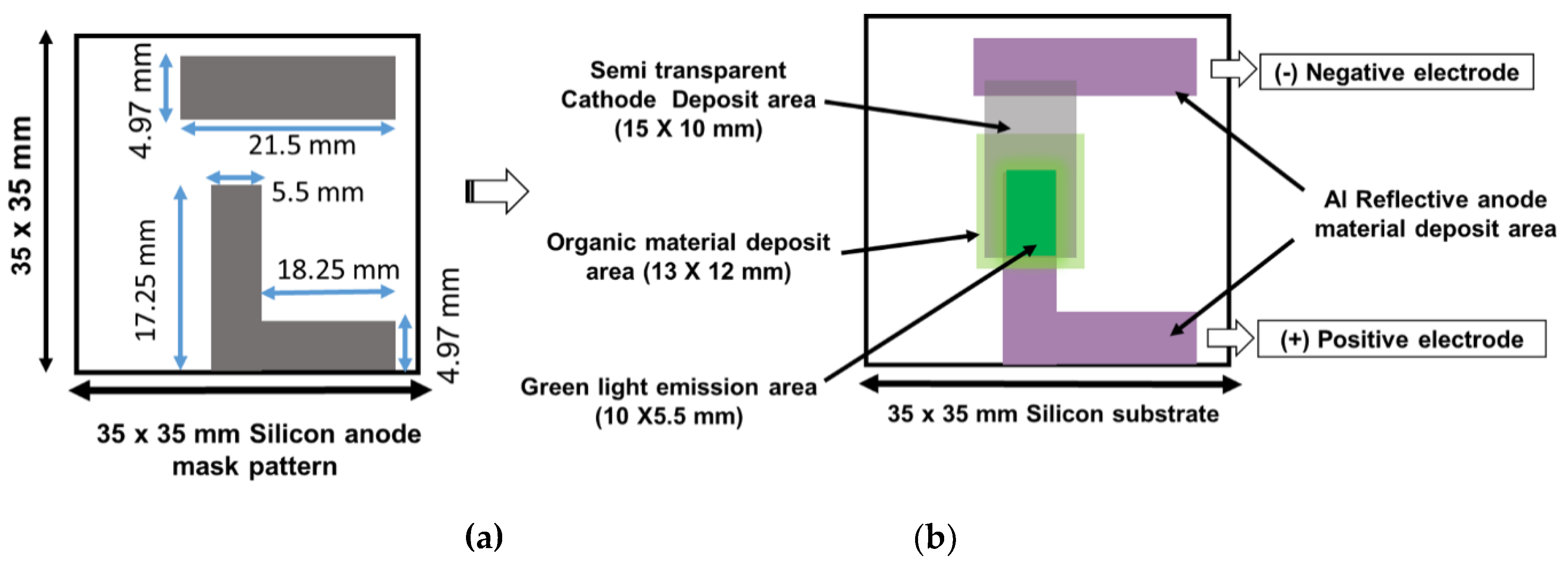
Figure 2.
Si-TEOLED (a) Energy band diagram; (b) Multilayer structural diagram.
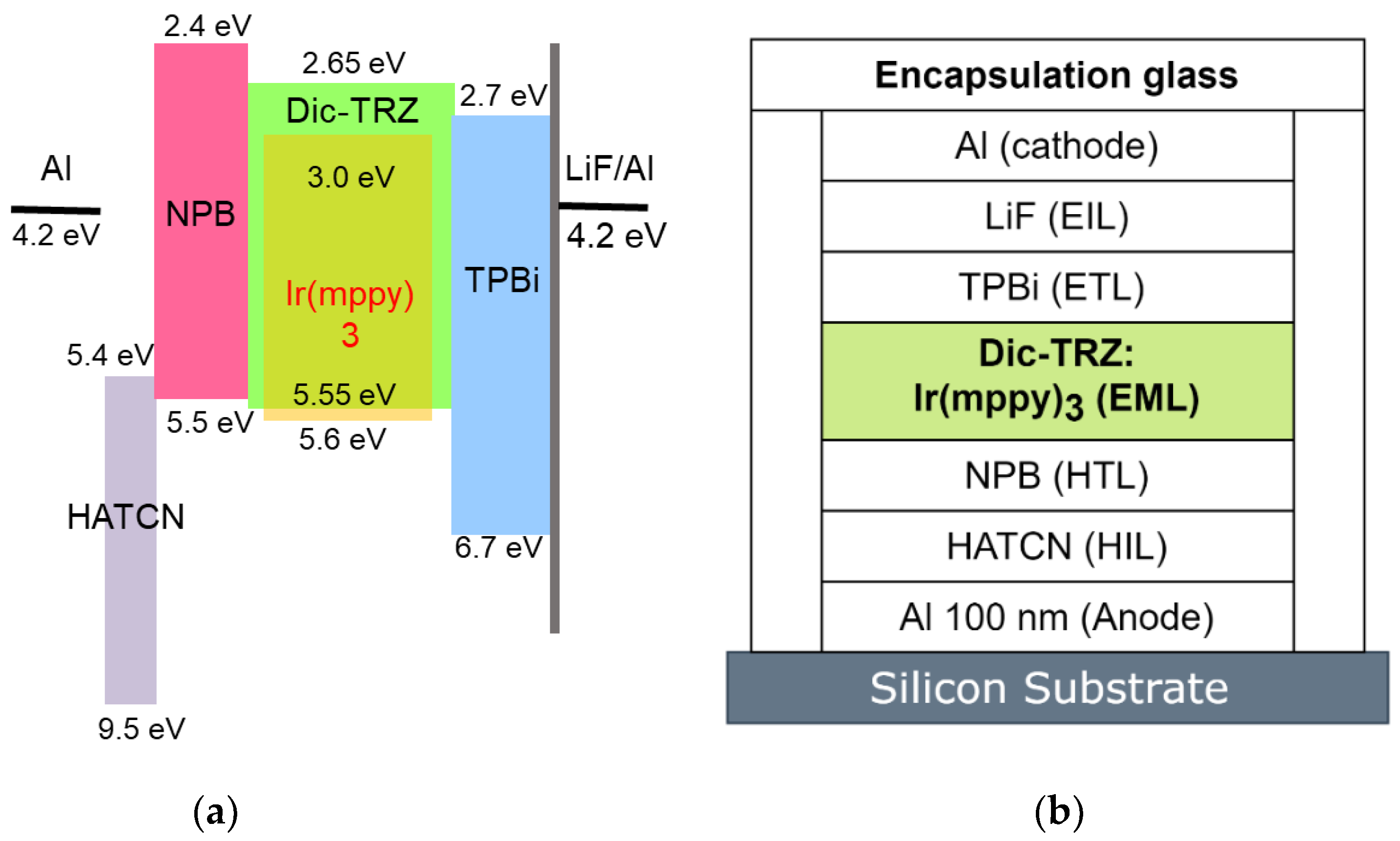
Figure 3.
Si-TEOLED encapsulation flow process.
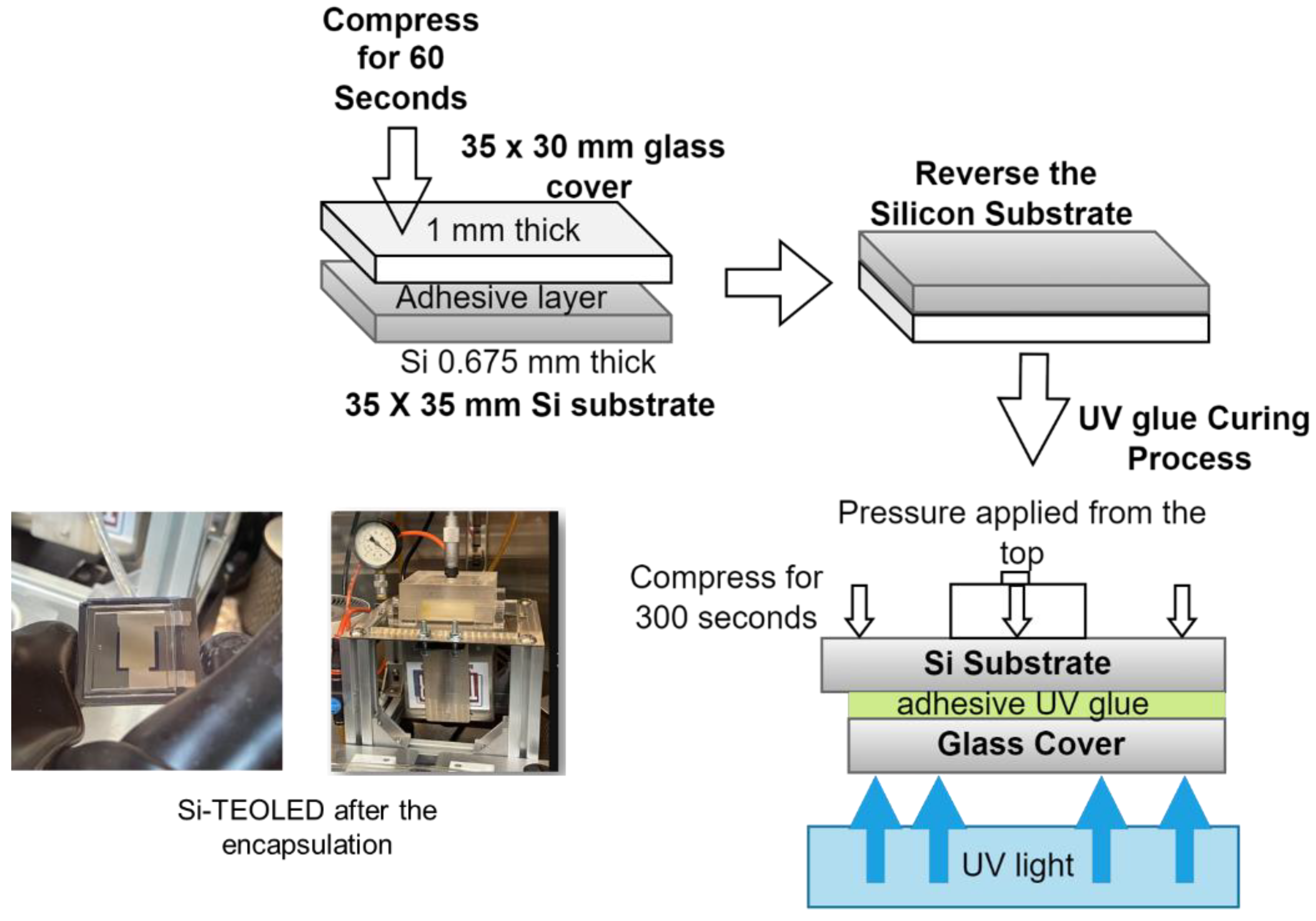
Figure 4.
Si-TEOLED lifetime measurement setup.

Figure 5.
(a) Transmittance (T); (b) Reflectance (R); and (c) Absorption (A) at different thicknesses of Al for the cathode layer.
Figure 5.
(a) Transmittance (T); (b) Reflectance (R); and (c) Absorption (A) at different thicknesses of Al for the cathode layer.
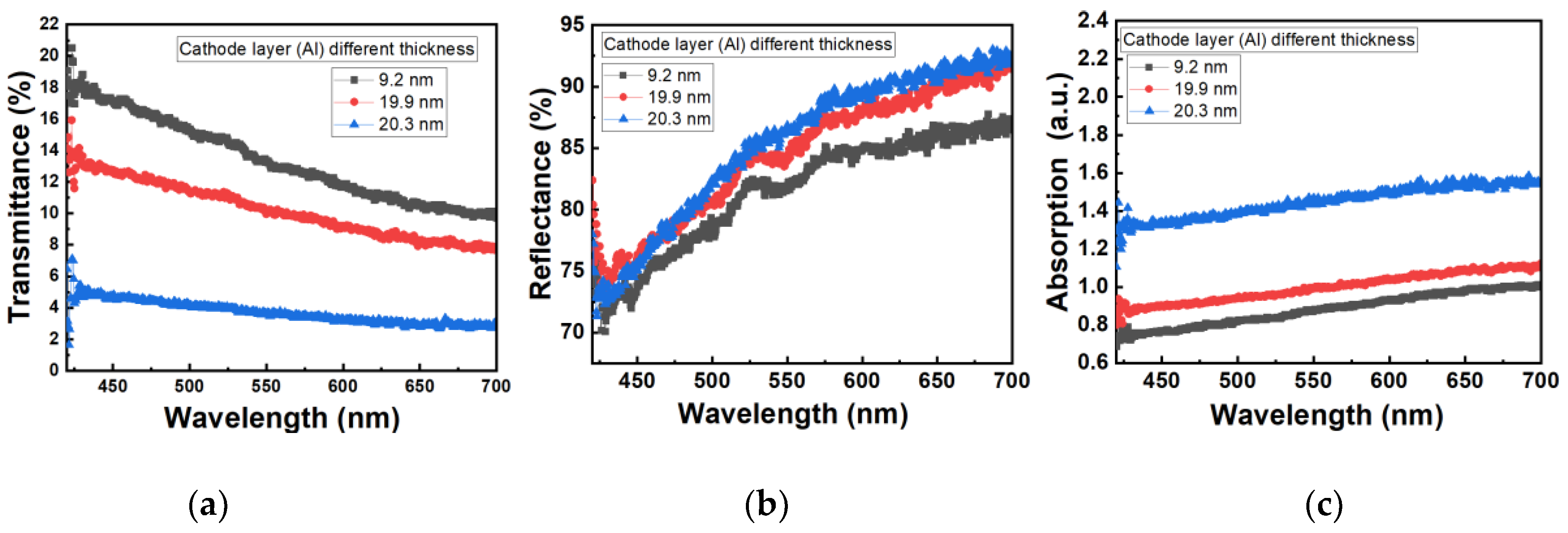
Figure 8.
2 D view of Anode layer surface AFM measurement.
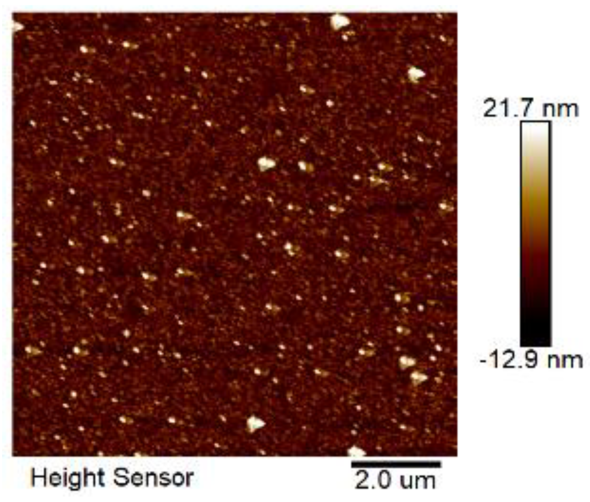
Figure 9.
SEM images of the Al anode layer at different magnified values, (a) x10,000, (b) x20,000.
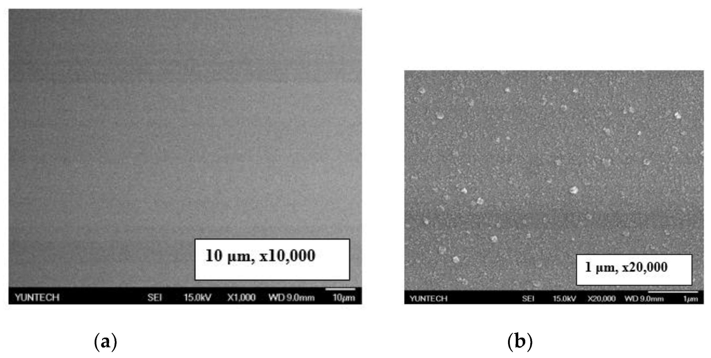
Figure 10.
Si-TEOLED devices with different dopant concentrations:. (a) J–V; (b) L–V; (c) Y-V; and (d) EL spectrum.
Figure 10.
Si-TEOLED devices with different dopant concentrations:. (a) J–V; (b) L–V; (c) Y-V; and (d) EL spectrum.
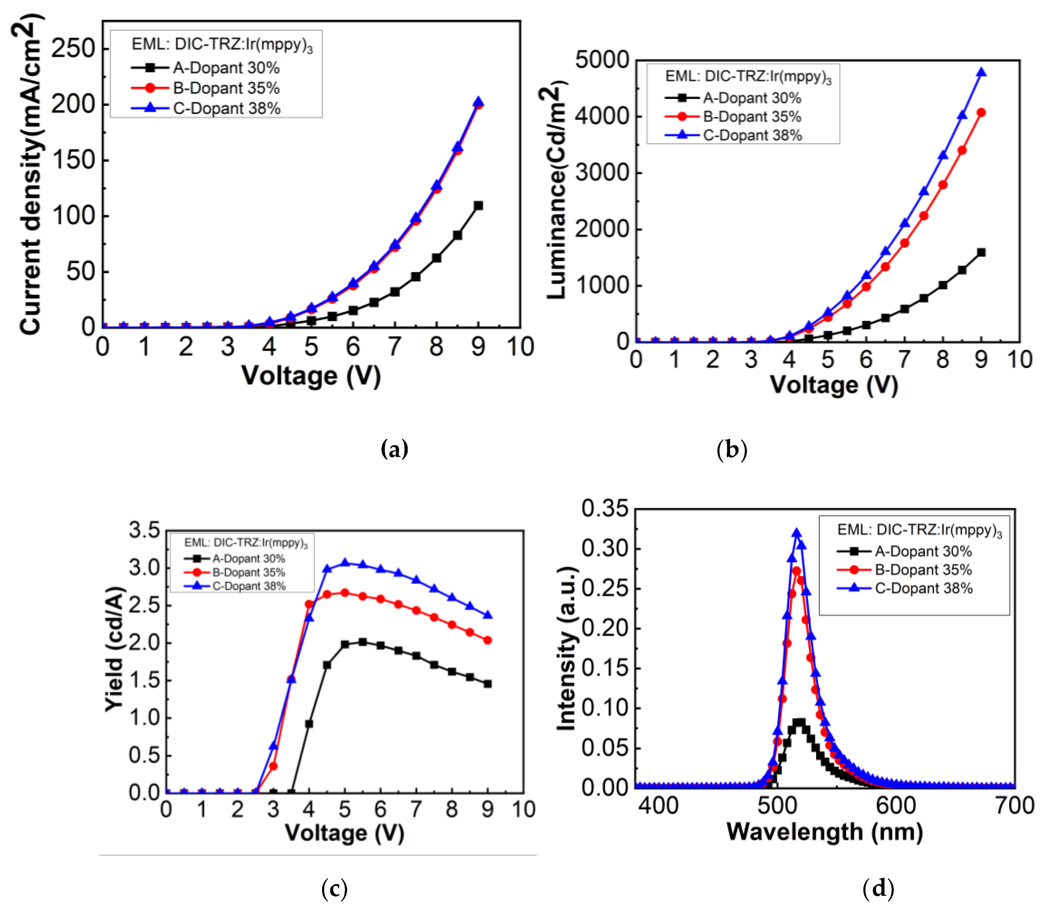
Figure 11.
Comparison of EL intensity of TE-OLED (Si), and BE-OLED (glass).
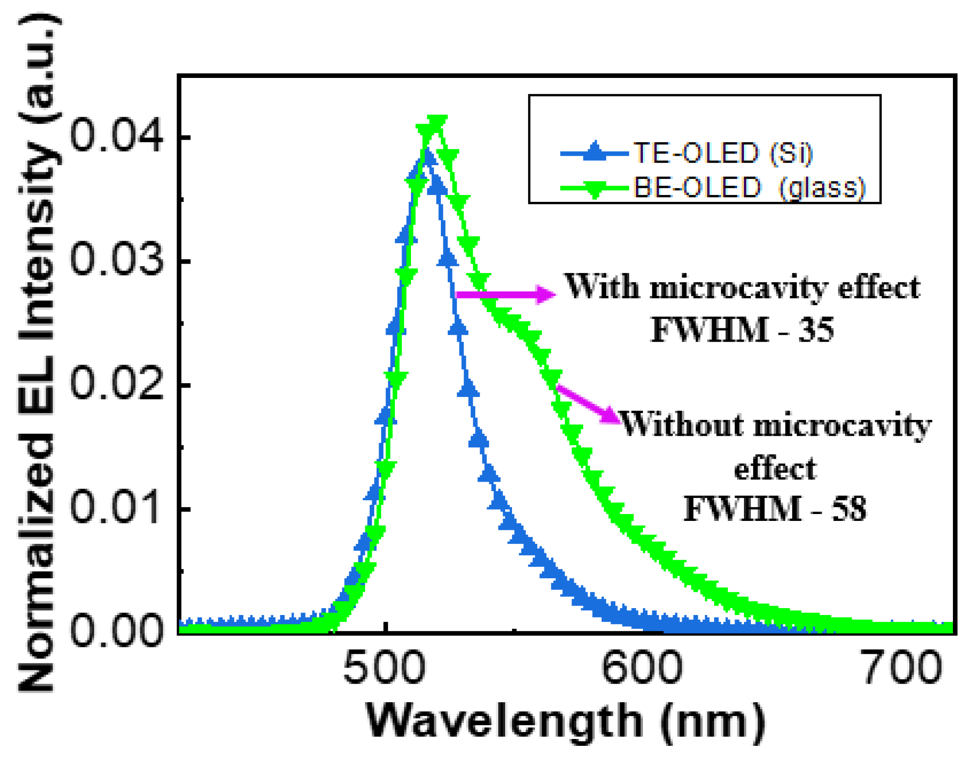
Figure 12.
Si-TEOLED device lifetime measurement with different dopant concentrations.
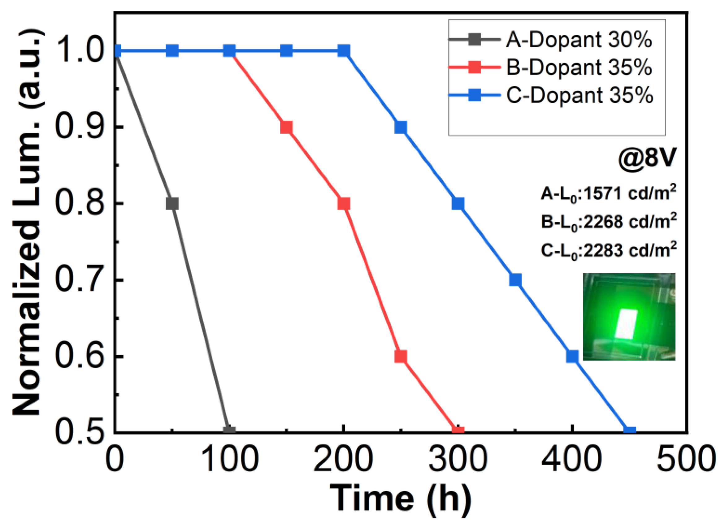
Figure 13.
Consistent emission area uniformity over time: (a) Day -1; (b) Day-5; (c) Day-11; and (d) Day-15. .
Figure 13.
Consistent emission area uniformity over time: (a) Day -1; (b) Day-5; (c) Day-11; and (d) Day-15. .
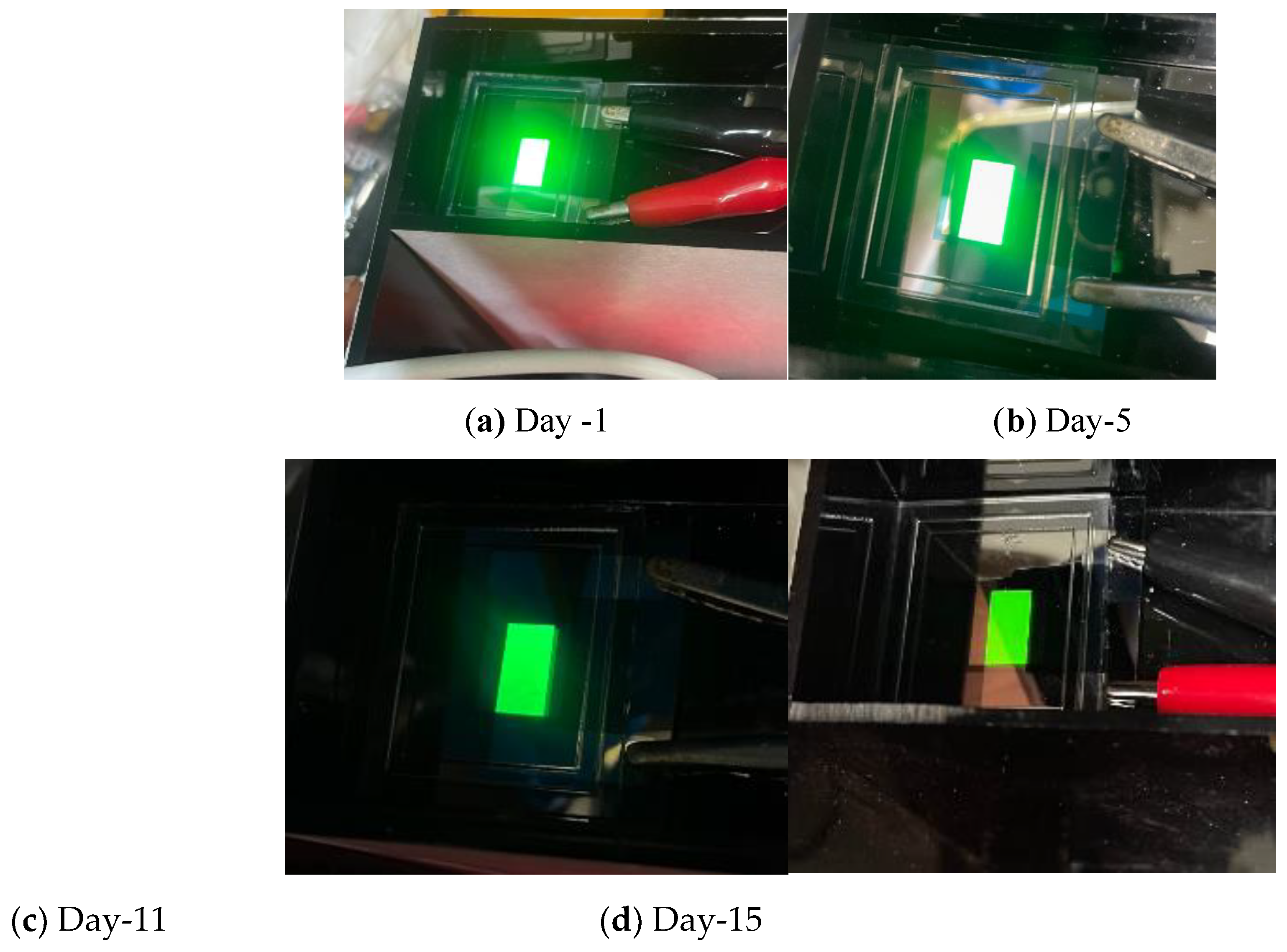
Figure 14.
Thermal image test: (a) Si-TEOLED applied with 8 V; (b) IR image After 200 seconds.
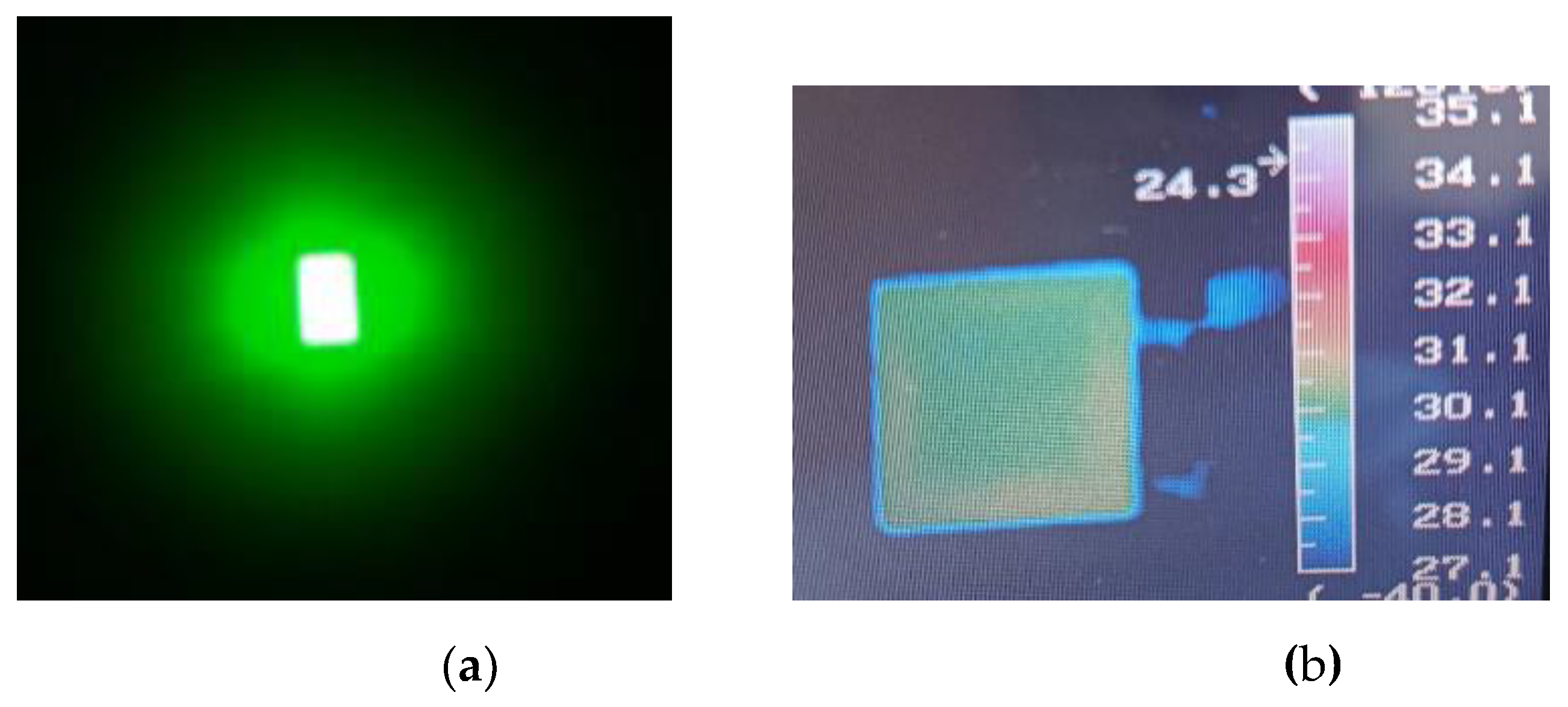

Table 1.
Transmittance (T), Reflectance (R), and Absorption (A) at different thicknesses of Al for the cathode layer.
Table 1.
Transmittance (T), Reflectance (R), and Absorption (A) at different thicknesses of Al for the cathode layer.
| Substrate | Cathode layer (Al) Thickness |
Transmittance (%) @ 550 nm |
Reflectance (%) @ 550 nm |
Absorption (a.u.) @ 550 nm |
|---|---|---|---|---|
|
Glass |
9.2 | 16 | 78 | 0.8 |
| 19.9 | 12 | 80 | 0.9 | |
| 20.3 | 5 | 83 | 1.3 |
Disclaimer/Publisher’s Note: The statements, opinions and data contained in all publications are solely those of the individual author(s) and contributor(s) and not of MDPI and/or the editor(s). MDPI and/or the editor(s) disclaim responsibility for any injury to people or property resulting from any ideas, methods, instructions or products referred to in the content. |
© 2024 by the authors. Licensee MDPI, Basel, Switzerland. This article is an open access article distributed under the terms and conditions of the Creative Commons Attribution (CC BY) license (http://creativecommons.org/licenses/by/4.0/).
Copyright: This open access article is published under a Creative Commons CC BY 4.0 license, which permit the free download, distribution, and reuse, provided that the author and preprint are cited in any reuse.


