1. Introduction
Photovoltaic (PV) energy is one of the most promising ways to meet the increasing global energy demand. For the wide application of PV energy, the voltage generated from a low-voltage PV panel must be boosted and supplied to the grid. There are several works done to implement double-stage power conversion [
1]. The voltage can be boosted separately to a required value, thus the inverter design and controller become much easier. However, it has a challenge, especially under high duty cycle operation conditions, which reduces system efficiency [
2,
3]. In addition to that, it has several drawbacks like higher complexity, higher cost, reliability issues, impact on the dynamic response of the system, bigger size, and heavier weight which led to the invention and subsequent advancement of single-stage voltage boosting using quasi-Z-source inverters (qZSI) [
4,
5,
6]. Using qZSI helps to reduce the circuit components which makes it highly compact. Voltage boosting and power inversion are possible in the qZSI due to the shoot-through (ST) in which all the switches in the same inverter leg can be short-circuited [
7]. However, it is not possible in double-stage power converters. The qZSI topology can be used for PV applications that do not require an input capacitor due to the continuous input current generated from the PV panels. There has been advancement in the topology of the qZSI and an advantageous one is to use the three-level topology, because it enables to harvest more energy with higher efficiency [
8].
Although much progress has been experienced with the implementation of three-level topology in PV systems [
9], there are still some limitations in terms of common mode voltage imbalance and leakage current flow [
10]. While, achieving the maximum power point (MPP) remains the most important issue using an appropriate algorithm[
11]. There are several novel maximum power point tracking (MPPT) algorithms proposed to track the MPP for PV systems. These algorithms perform well, especially under partial shading conditions (PSCs) caused by shading of trees, buildings, dust, passing clouds, snow, and bird droppings [
12,
13]. Partial shading (PS) affects the performance and characteristics of PV panels, by producing multi-peaks of MPP in the power–voltage (P–V) and current-voltage (I–V) curves. Traditional MPPT algorithms such as perturb and observe (P&O), hill climbing, and incremental conductance cannot operate at global maximum power point (GMPP) as they drift around the first maxima which may not be the GMPP. To overcome this issue, several optimization techniques such as the genetic algorithm (GA), particle swarm optimization (PSO), ant colony optimization (ACO), artificial bee colony, and gray wolf optimization (GWO) have been proposed [
14]. These techniques can track the optimal MPP of the PV array when shading occurs. However, the efficiency is degraded as the operating point of the PV system moves away from the local maxima to obtain global maxima. To address this issue with optimized efficiency and better performance, the P&O algorithm can be modified to reduce the number of MPPT controllers. Reducing the number of MPPT controllers provides additional advantages like reduced cost and complexity.
Moreover, higher boosting is needed for grid-connected low-voltage PV modules to match the required AC voltage in the grid [
15]. Three-level neutral-point-clamped quasi-Z-source inverter (3L-NPC-qZSI) is mostly used for higher voltage boosting which can be supplied to the grid with improved power quality [
16]. In addition, the number of components used in the inverter topology is also reduced [
17]. Also, 3L-NPC-qZSI merges the strengths of a two-level topology, like reduced conduction losses and simplicity, with the benefits of a three-level topology. This makes it a viable option for specific low-voltage applications and also to connect with the grid because of its higher boosting ability [
18].
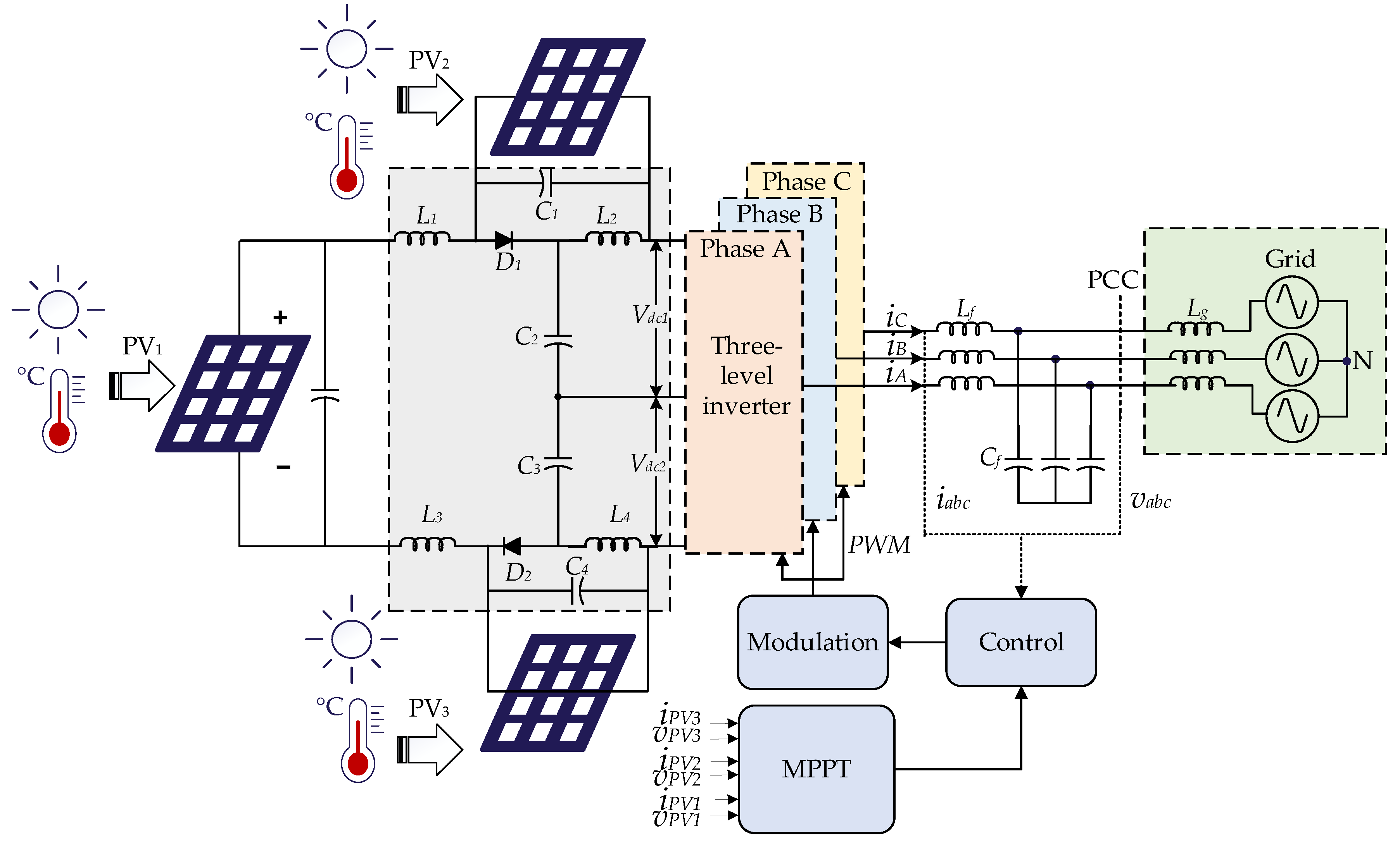
In this paper, a triple-input three-level neutral-point-clamped quasi-Z-source inverter (TI-3L-NPC-qZSI) is developed as shown in
Figure 1. The three-level inverter topology is selected because of its ability to provide high quality power output. The main focus of the paper is to design such a highly efficient and robust rooftop PV system while harvesting maximum possible energy from multiple PV input with lower input voltage. In addition, more energy can be harvested with multiple PV inputs which utilizes one MPPT controller, resulting in a more cost-effective solution.
The rest of this paper is organized as follows:
Section 2 presents the proposed PV arrangement for the TI-3L-NPC-qZSI topology and its operational conditions.
Section 3 performs dynamic modeling and small signal analysis to ensure that the proposed system is stable, reliable, and operates efficiently.
Section 4 presents the topology's parameter design.
Section 5 illustrates the implemented MPPT algorithm.
Section 6 presents the simulation results and discussion.
Section 7 compares the implemented topology with other similar topology proposed in the literature.
Section 8 concludes the paper.
2. System Description
The proposed novel arrangement is presented in
Figure 1, in which, additional two PV arrays, PV
2 and PV
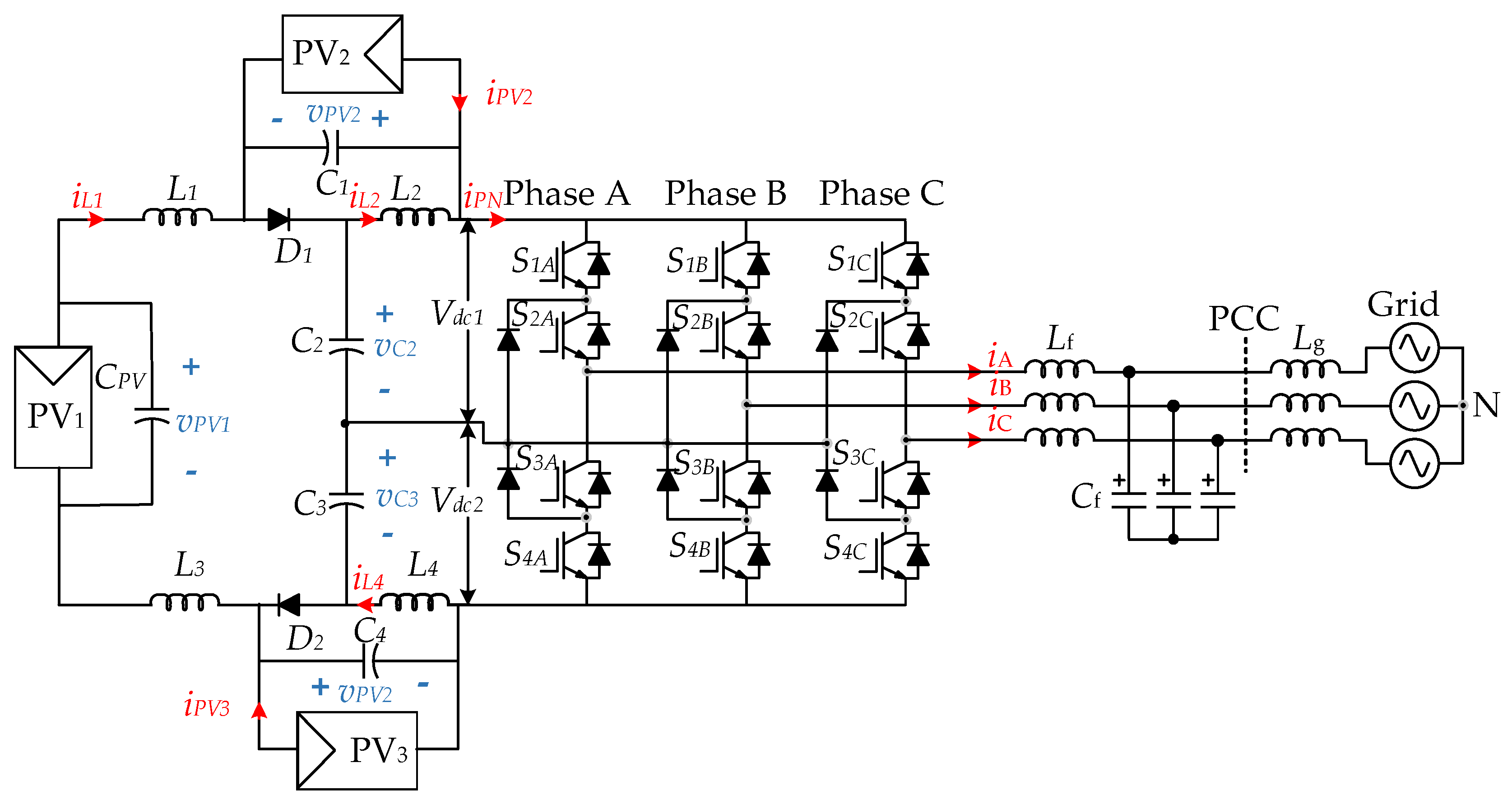
3, have been added into the upper and lower quasi-Z-source (qZS) network. The upper qZS network has 2 inductors, 2 capacitors and a diode. Similarly, the lower qZSI is a replica of the upper qZS network. The current and voltage of all three PV panels are sensed for the MPPT controller and the grid voltage and current is sensed for the ac controller. Finally, the generated pulse width modulation (PWM) signal is fed to the inverter switches. The state of these switches decides the operation mode of inverter. The detailed circuit for the TI-3L-NPC-qZSI topology is shown in
Figure 2.
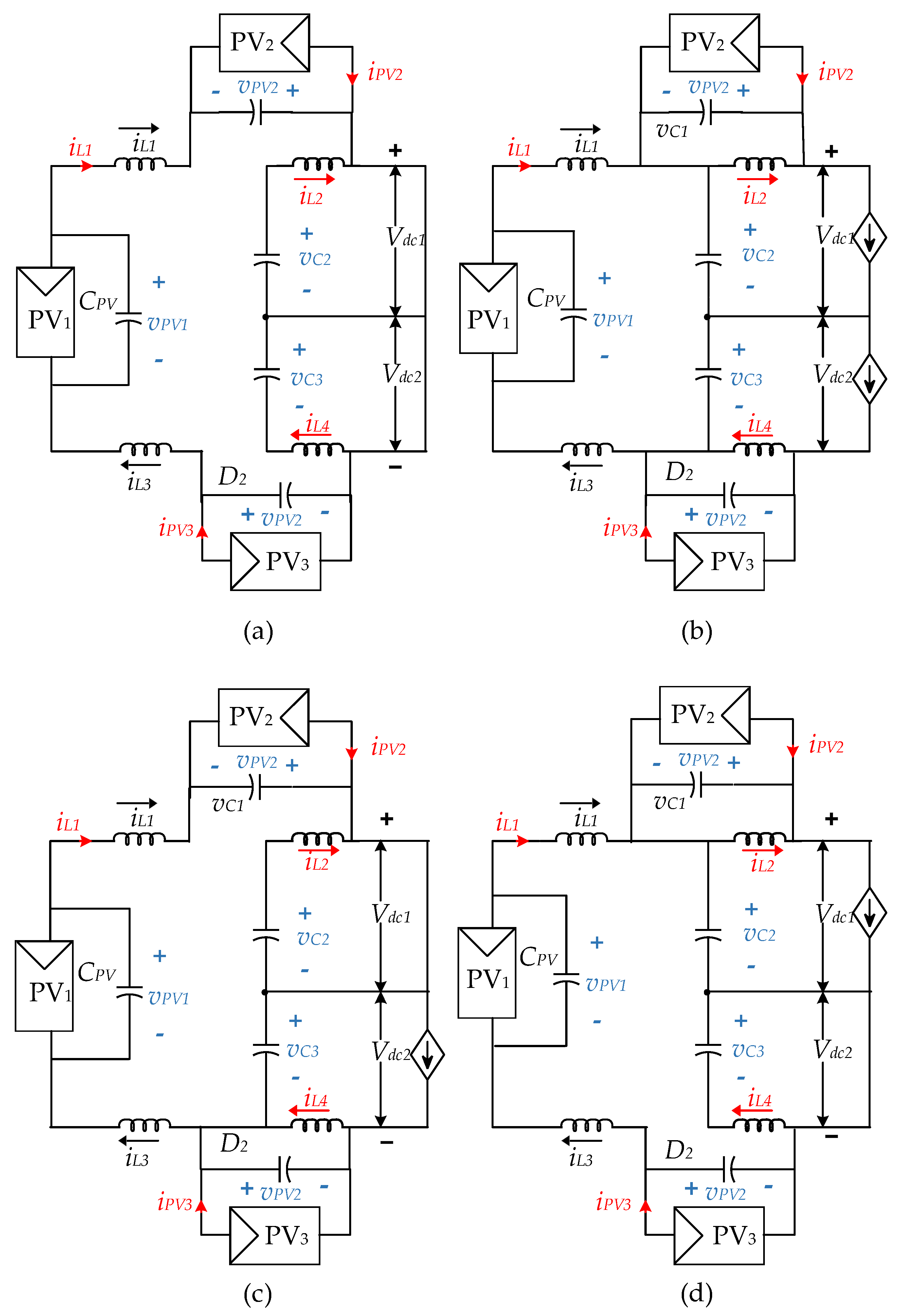
To investigate the TI-3L-NPC-qZSI, the equivalent circuits of the converter during full-ST (FST), non-ST (NST), upper-ST (UST) and lower-ST (LST) are presented in
Figure 3. During the FST, as illustrated in
Figure 3(a), one of the converter legs is short-circuited, increasing the current in the impedance network as the capacitor discharges, moving the PV array's operating points closer to their short-circuit currents. According to
Figure 3(a), the energy stored in C
PV is released to L
1, whereas the energy of C
2 and C
3 are discharged into L
2 and L
3, respectively. Similarly, as shown in
Figure 3(c) and 3(d), for the UST and LST, the upper and lower two switches will be short circuited respectively. Capacitor voltage is discharged in both of the ST state. After the ST, when the active state starts, the capacitors charge again until the inductor current is finished. As shown in
Figure 3(b), PV
1, L
1 and L
3, boosts C
2 voltage and C
3 voltage. And, PV
2 and L
2 boosts C
1 voltage. Similarly, PV
3 and L
4 boosts C
4 voltage. The generated power is simultaneously supplied to the grid through the TI-3L-NPC-qZSI.
3. Dynamic Modelling
The small signal analysis and modelling are carried out with the following assumption:
The inductances and capacitances of qZSI are equal and indicated as L and C, respectively
Continuous conduction
Lossy capacitor and inductors with resistance RC and RL, respectively
Diodes and switches are ideal
During the ST state (), energy stored in capacitors is transferred to inductors and during NST state (), sources (i.e., PV panels) charge the capacitors and supply the load, as input diodes conduct. Inductors are discharged through loads and thereby boosts the DC-link voltage. The total switching time () is the sum of ST and NST states, i.e. = +. State vector () is formed using the currents of inductor L1 () and L2 () and the voltages of the capacitor C2 () and PV2 (). Similarly, the input vector () is formed using the voltage of PV1 (), the current of PV2 () and the DC-link current (iPN).
The state vector is
And, the input vector is
Subsequently, the state space equation in ST and NST modes are obtained as
where
Using (3) and (4) over a complete switching cycle of
for average, the average state-space model can be obtained as
in which
,
,
is the ST duty ratio, and
is NST duty ratio with
, and
The small signal model of the proposed TI-3L-NPC-qZSI can be obtained by applying the Laplace transform on (3) and (4), with the introduction of perturbation on
,
and
. Each of these signals is substituted with addition of the equilibrium point and induced perturbation, i.e.,
, which finally induces
. The transfer function from
to
is used in investigating the system stability and parameter design. The assumption made for the analytical calculation of the transfer function include
,
,
,
,
.
where
. The transfer function from
to
,
can be obtained by converting the formula obtained by Kirchhoff’s law applied to the input of the TI-3L-NPC-qZSI into the Laplace domain
Accordingly, the block diagram of the closed-loop control of TI-3L-NPC-qZSI model in the Laplace domain can be obtained as shown in
Figure 4. The transfer function
is derived similarly as it is for a basic qZSI topology [
19]. However, the relationship of inductor current varies. Taking the relation from (5), the relation of all the inductor currents can be derived as
=
-
and
=
-
.
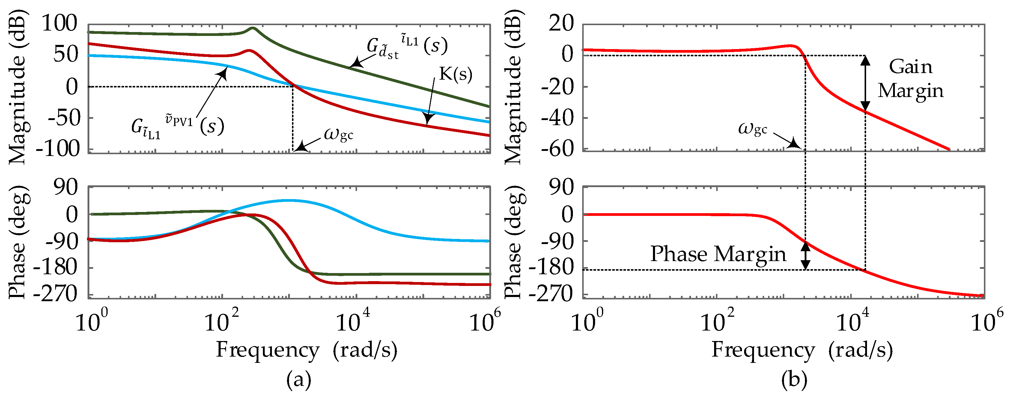
The Bode plots of the obtained transfer functions
and
with their product K(s) (being the transfer function from the duty cycle, i.e.,
to the PV voltage
) are shown in
Figure 5(a), which shows the gain crossover frequency (
being 1100 rad/s. And,
Figure 5(b) suggests
of 999 rad/s, phase margin of 80
and gain margin of 37 dB to the corresponding closed-loop frequency response.
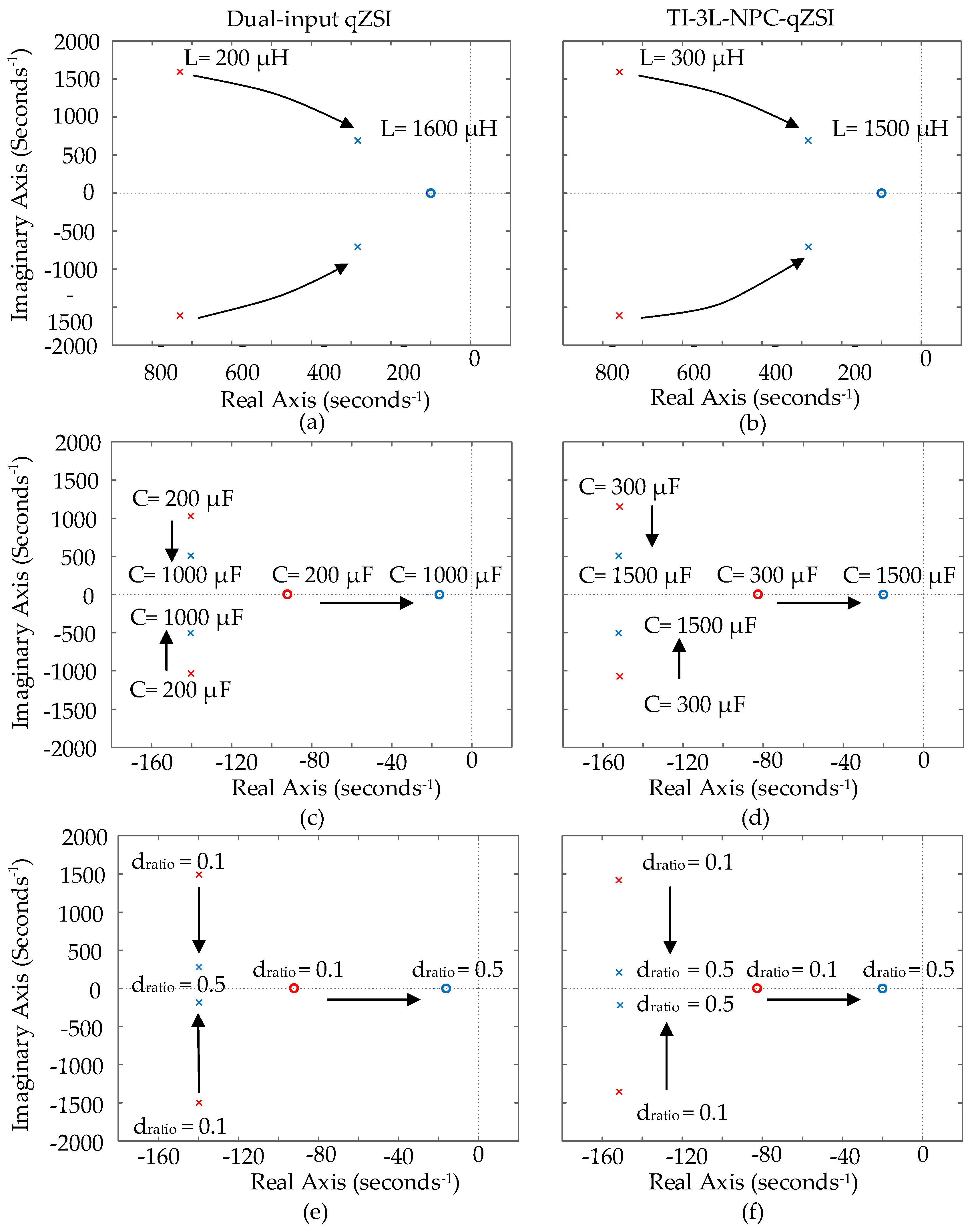
The root loci of the transfer function
is shown in
Figure 6. Values for inductor, capacitor and ST duty ratio is increased in the direction of arrow and the dynamic characteristics are observed. The system is designed with the parameters being
= 73 V,
= 5 A,
= 0.25,
C1,2 = 1.5 mF,
L1,2 = 1.5 mH
RC =
and
RL =
. The proportional (
kp) and integral (
ki) gains of
are taken as 0.1 and 45, respectively, and for
are taken as 0.05 and 2, respectively. When the root loci of the TI-3L-NPC-qZSI is compared with the root loci of the dual-input qZSI, the stability of both the systems is observed to be equally fine [
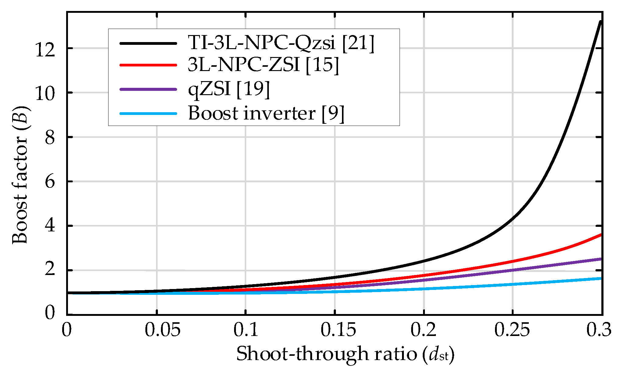
20]. Poles and zeros are on the left half plane. The closed-loop system is stable and in addition to that its boosting ability is the best among its competing converter topologies. Comparison of the boost factor with those topologies is shown in
Figure 7. Hence, this topology is promising among various converter topologies [
9], [
15,
19,
21]. The design of this topology is performed in next section.
4. Design of the TI-3L-NPC-qZSI Topology
Inductors are designed in such a way that it is able to limit the current during the ST process. Using (4), the desired relationship for inductors can be derived [
5].
where
is the switching frequency,
is the number of ST states that happen in one switching period,
is the maximum ST duration.
Capacitors absorb the currents going through the diode (D) during the active state, which is, according to
Figure 2(c) and Kirchhoff’s current law, estimated as
The capacitance of all capacitors (
) must be equal in order to avoid resonance in the qZS-network [
22]. The feature of these capacitors includes the filtering of high frequency ripple caused by switches and low frequency caused by oscillatory instantaneous power. From (11) and (12), the capacitor values can be designed as
where
are the allowable ripple voltage for PV
1, PV
2, PV
3 and
is the grid frequency.
Additionally, the PV parameter is of importance. Using (4) and equating it with zero for steady state condition gives
It is obvious in (14) and (15) that the duty ratio is greater than zero. Hence, and when = 0.25, is double of . There are other things to be considered while designing the topology. The power generation from PV1 must be greater than the other two to ensure . The power generation from PV2 and PV3 should be equal to . And, in order to balance the neutral point voltage, and from PV2 and PV3 panels should be equal.
5. Modified MPPT Algorithm
Achieving maximum power is the most critical, challenging and an important task at the same time. The main objective is to reduce the complexity and cost by using only one controller to control three PV panels.
In order to optimize the power generated from the PV panel, one must track the maximum power generated by the panel and achieve it using an efficient algorithm. Several MPPT algorithms have been reported [
14,
23,
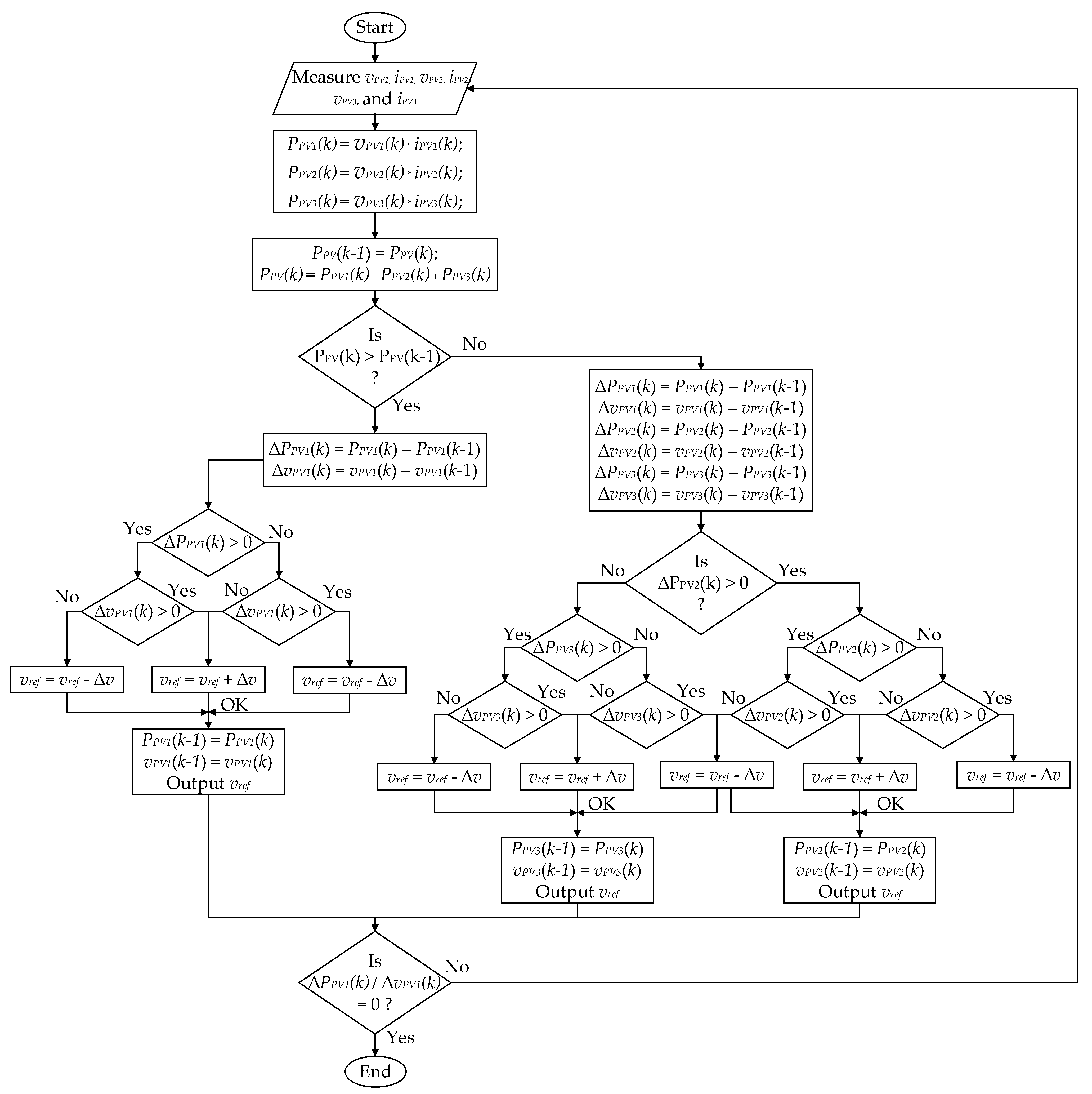
24] to solve the issues. The P&O algorithm is preferred because of its cost-effectiveness. Moreover, to optimize and track the maximum power generated by three panels connected to a single converter needs some modifications in the control algorithm. Therefore, a modified P&O algorithm is implemented to the proposed topology (see
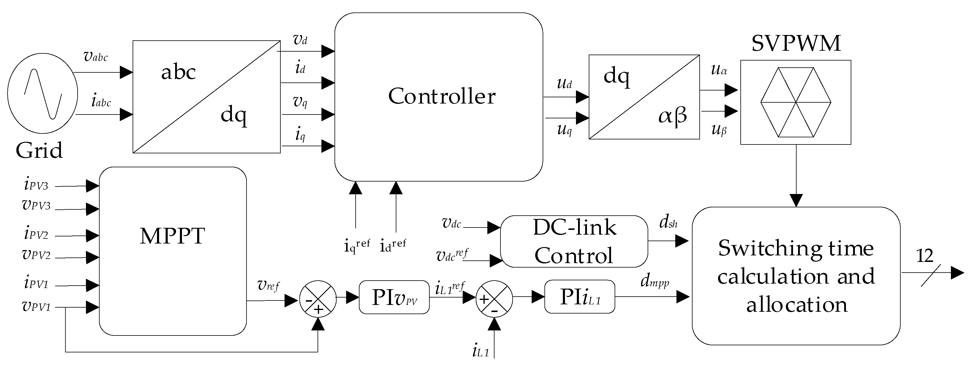
Figure 1), and the flowchart of the modified MPPT algorithm is presented in
Figure 8. The sampling frequency of the MPPT controller is set to 20 Hz and the increment
∆v is taken as 1 V for the perturbation. The perturbation on PV
1 has effect on the other two panels. Hence, both the panel’s observation process is based on the perturbation of PV
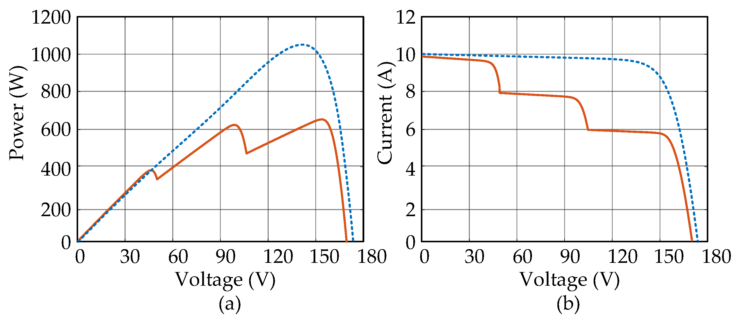
1 and with themselves as well. Due to this, separate MPPT controllers are not appropriate. As such, a single MPPT controller with the ability to track the maximum power by considering the impact of perturbation on each other, is implemented in the following. As shown in
Figure 9, the MPP is achieved with the modified P&O algorithm shown in
Figure 8 during standard test conditions (STCs) and PSCs with PV1 at 600 W/m
2, PV2 at 800 W/m
2, and PV3 at 1000 W/m
2. The modified P&O works basically by perturbing the operating voltage and observing the power variation. This leads the operating point towards the MPP.
The MPP can be tracked when the following condition is achieved:
The fluctuations in voltage of both the panels PV
2 and PV
3 are used in the same sampling period for the self-perturbation of PV
2 and PV
3. The correct tracking direction is decided according to the change in the reference voltage in the positive or negative direction. Similarly, the perturbation with respect to PV
1 is performed in an alternative sampling period. Here, the change of the reference voltage is governed by two closed-loop controls, as shown in
Figure 10:
However, both the self-perturbation and perturbation with respect to PV1 is performed. The one with the higher impact on the reference voltage is selected to achieve the MPP faster. Finally, the MPPT controller generates a reference voltage which is used to obtain the ST ratio at the MPP which is utilized to calculate the switching time.
6. Simulation Results and Discussion
The PV system as depicted in
Figure 1 is built in MATLAB and the simulation work is performed based on the parameters shown in
Table 1. The panel PV
1 has two strings with two series modules and both PV
2 and PV
3 panels have a string with a single module. Initially, the simulation is performed at STC and after that, different irradiance for PV
1, PV
2, and PV
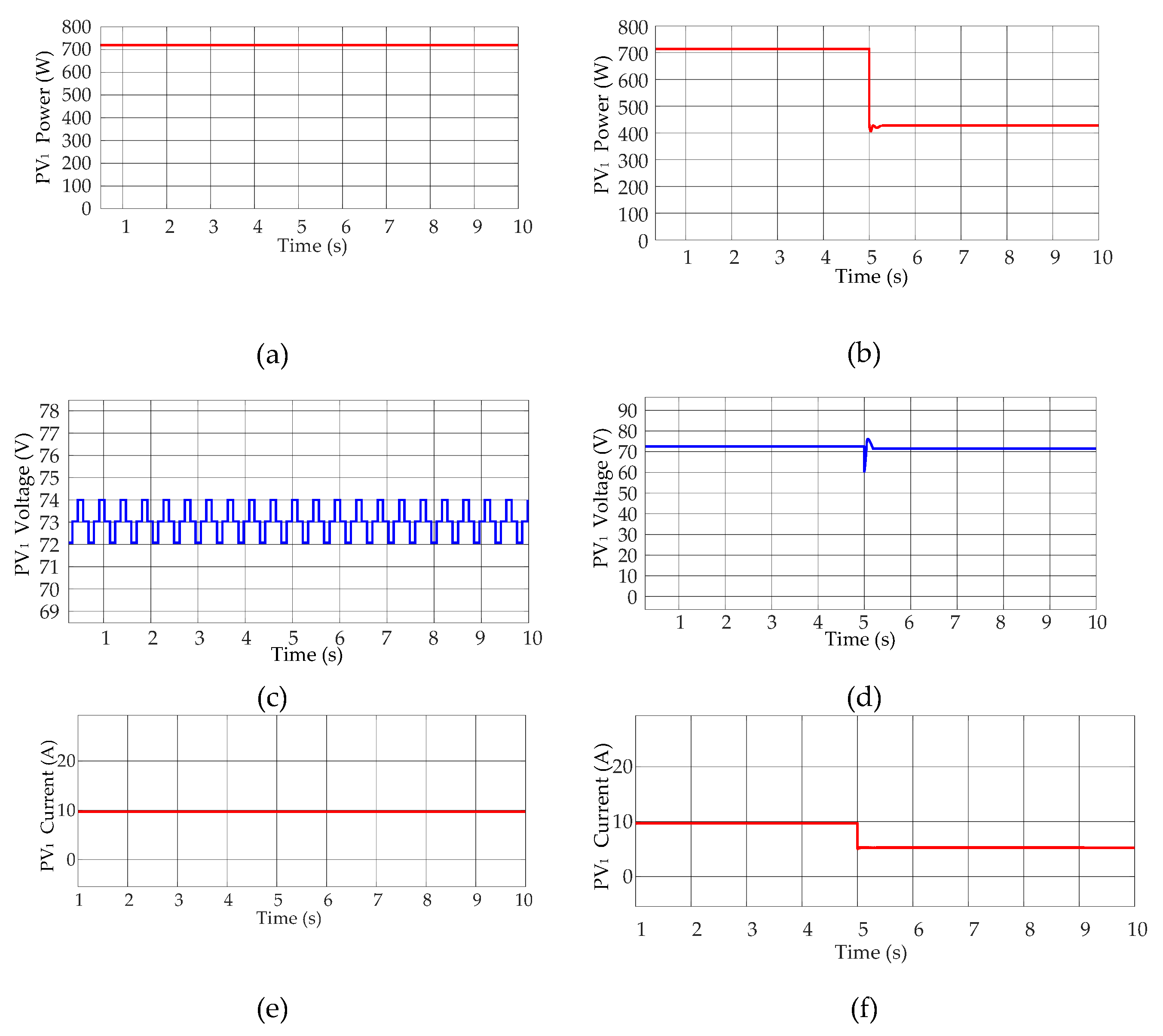
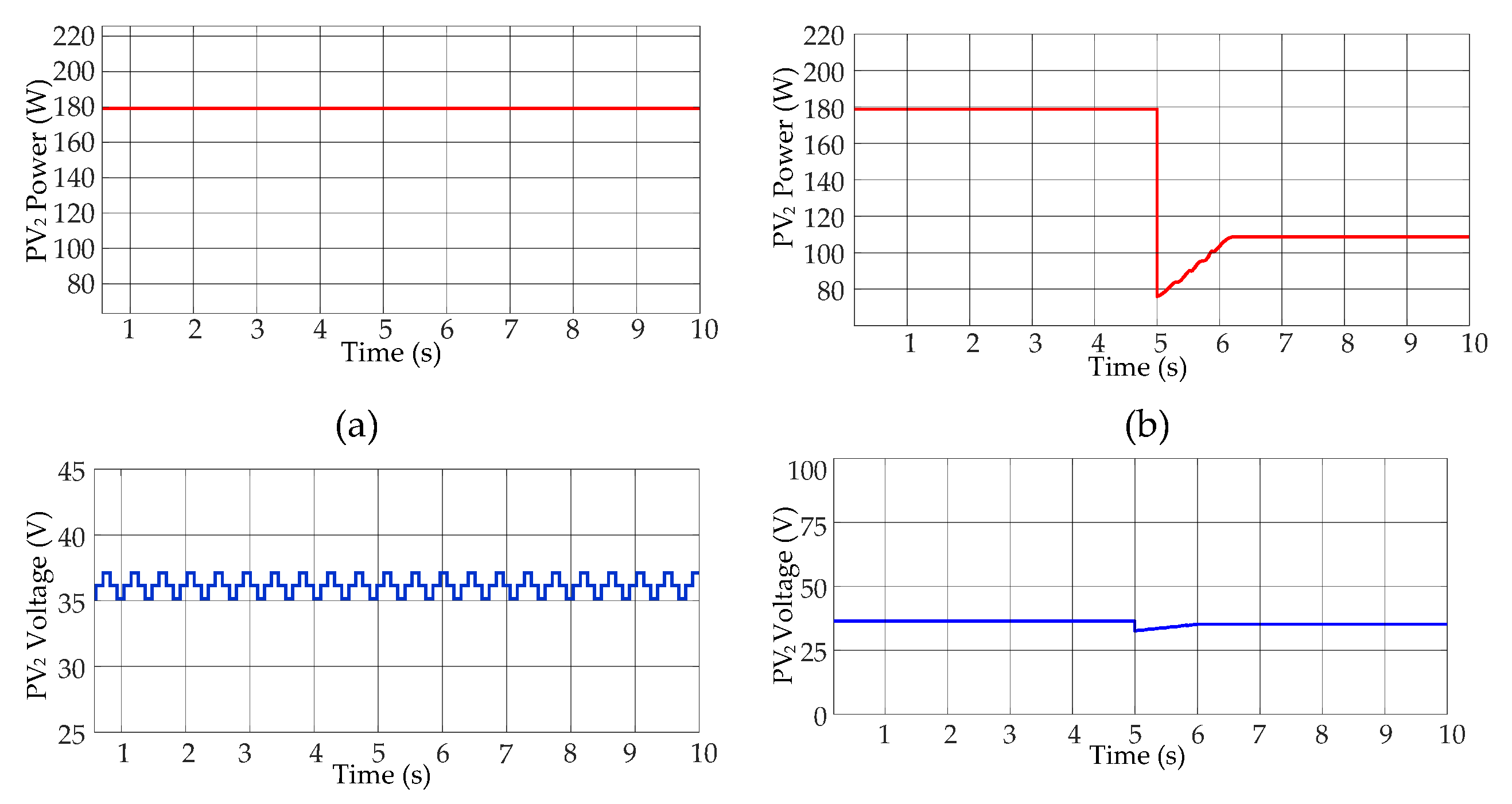
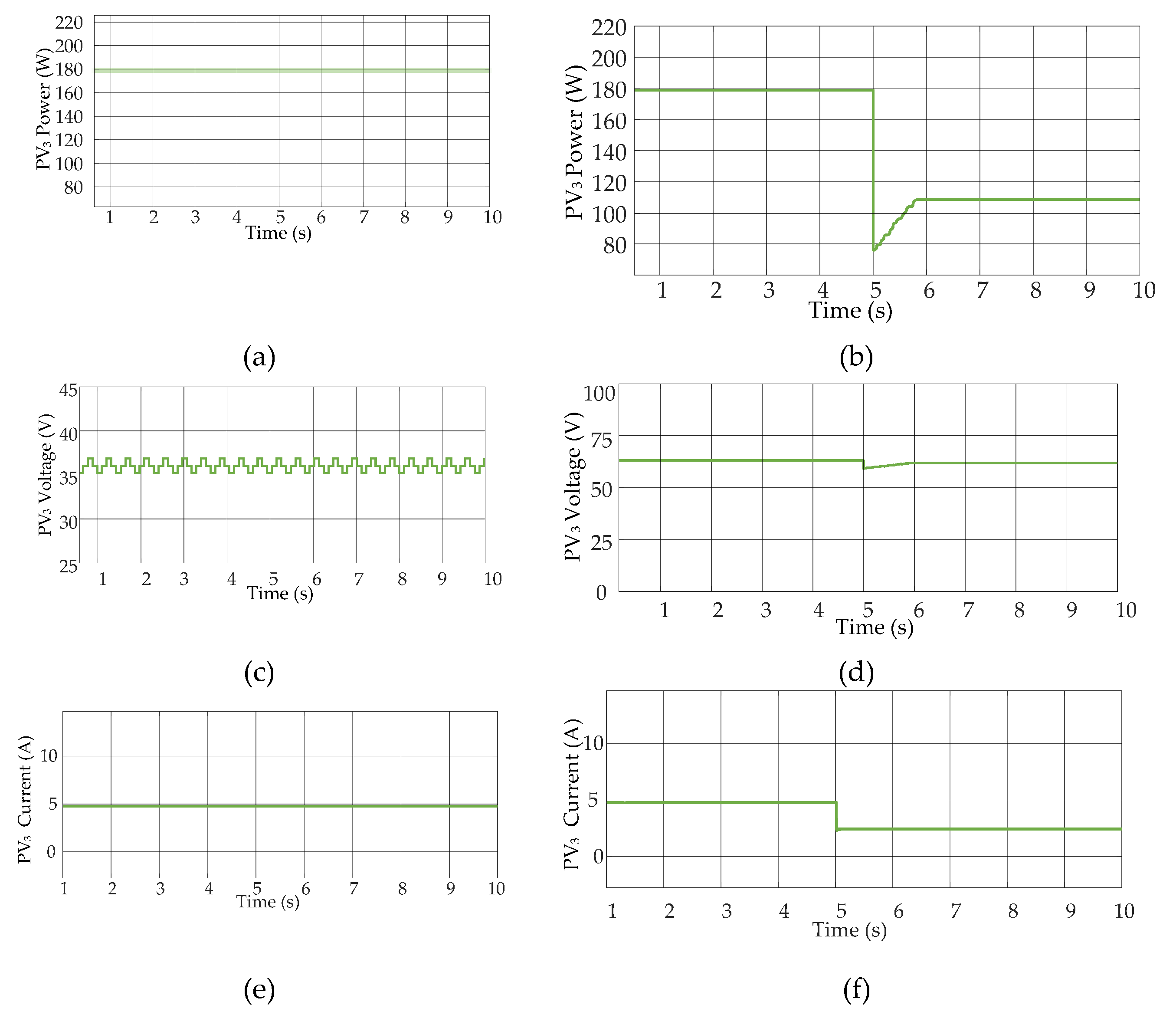
3 is taken into consideration to explore its impact on the power generation. Simulation results are shown in
Figure 11,
Figure 12 and
Figure 13 for PV
1, PV
2 and PV
3 respectively.
It has been taken care that the power generation from PV
1 must be greater than both of the other panels and the identical panel rating is used for PV
2 and PV
3 because the generated voltage from these panels must meet the criteria as discussed in
Section 4. From the simulation results, it is observed that the change in irradiance on the first PV array affects power generation in all other PV arrays and the power generation of PV
3 is also affected by PV
2. The power ripple during the steady state is of 2 W. Also, the power value achieves the steady state quickly which shows that the controller provides fast dynamics. PS is encountered in PV
2 while there is no shading on PV
3, and to balance the neutral point voltage and to balance the capacitor voltage, the power generation of both panels are limited to the generation of PV
2. As obtained from the simulation results, the power achieved during STCs and PSCs has been presented in
Table 2.
The theoretical value of the power for a single module at STCs is tabulated in
Table 1. Comparing the theoretical value of power with the achieved maximum power values, the efficiency can be calculated [
25] as
where
represents the MPPT efficiency,
represents theoritical maximum power, and
represents the achieved maximum power. The highest MPPT efficiency of 99.2 % is achieved during STCs and the maximum conversion efficiency of 97 % is achieved during PSCs for the presented PV system with the modified P&O MPPT algorithm.
7. Comparative Analysis
In
Table 3, the comparison of the implemented topology with the other topologies that are already proposed by various researchers is presented. The comparison is done in terms of the number of MPPT controllers used (
NMPPT), number of PV input used to harvest energy (
Ninput), number of phases (
NP), component count, inverter level, energy harvesting, controller cost, switching frequency (
fs) as well as weather it uses neutral point clamped (NPC) inverter or not (for better power quality). In [
19], a voltage fed two-level qZSI has been presented for PV systems connected to the grid. In [
26], two PV inputs have been used to harvest maximum energy utilizing a unique three-level inverter topology which is the combination of two DC-DC buck-boost converter. In [
27], a grid-connected 3L-NPC-qZSI is utilized to harvest energy from a single PV input. In [
20], a grid-connected two-level qZSI is utilized to harvest energy from two PV inputs. While comparing all of these inverter topologies with the TI-3L-NPC-qZSI, it is clear that the number of MPPT controller can be minimized for multiple PV inputs according to the system requirements without affecting the overall performance of the PV system.
To assess the overall enhancement in performance of a PV system when utilizing different MPPT algorithms, a qualitative comparison can be conducted based on factors such as steady-state power ripple, MPPT control response dynamics, fill-factor (FF), mismatch losses, system complexity, and MPPT efficiency, as shown in
Table 4. Steady-state power ripple is the fluctuation of power allowed in the steady state value of the maximum achieved power. Power ripple can be limited to a small value while designing the MPPT controller. Similarly, the dynamics of the system must be faster to quickly achieve the MPPT. In addition, the FF is the measure of efficient energy conversion and the PSCs in the PV causes the variation in the FF. The FF is another factor used to study the power losses during the influence of shading for PV systems. The FF is determined as
where
is the percentage fill-factor,
is the maximum power,
is the open circuit voltage, and
is the short-circuit current.
Similarly, mismatch losses are evaluated by identifying the variance between the power achieved at the full irradiance and the power achieved at PSCs. It is determined as
in which
is the percentage mismatch loss,
is the power achieved at the full irradiance, and
is the power achieved during PSCs.
The complexity in the MPPT control can be made lower by using only one variable for perturbation but the complexity increases if more than one perturbation variables are used to observe the power variation. In the modified P&O MPPT algoritm in this paper utilizes voltage reference as a perturbing factor to observe the variation in power output.
The performance of the proposed topology is observed to be equally good as the dual-input qZSI based on the qualitative comparative analysis in
Table 4. The quantitative and qualitative comparison between other topology proves that the grid-connected TI-3L-NPC-qZSI can efficiently harvest optimum energy from three PV inputs using a single MPPT controller.
8. Conclusion
A dynamic modeling and small signal analysis of TI-3L-NPC-qZSI were performed. The small signal modeling of this topology is used to ensure system stability. The usage of three PV inputs does not increase the number of passive and active elements, being cost-effective. In addition, the size of passive elements is not larger than in standard qZSI topologies. The relationship between the voltages and the currents of three PV inputs is derived from the small signal modeling, which shows that the voltages of PV2 and PV3 must always be equal, and the power of PV1 must be greater than the other two, and thus the current generated from PV1 is higher.
The primary focus of the work was to understand the feasibility and application of a low-voltage rooftop PV system utilizing TI-3L-NPC-qZSI topology. It is not easy to achieve the MPP when using three panels. Therefore, a modified MPPT algorithm based on the perturb and observe concept is used to address this issue. This idea is cost-effective as it uses only one MPPT controller. Based on simulation results, it can be confirmed that the control arrangement and design topology can perform well in power mismatch scenarios. The low voltage generated from the PV system is boosted and power with good quality is supplied to the grid. In a nutshell, the use of a single MPPT controller for three PV panels for a rooftop PV system is proposed in this article.
Author Contributions
Conceptualization, B.G. and Y.Y.; methodology, B.G.; software, B.G.; validation, B.G., Y.Y., A.M.A. and R; formal analysis, B.G.; investigation, B.G.; resources, Y.Y.; data curation, B.G.; writing—original draft preparation, B.G.; writing—review and editing, B.G., Y.Y., A.M.A. and R; visualization, B.G.; supervision, Y.Y. All authors have read and agreed to the published version of the manuscript.
Funding
This research received no external funding.
Data Availability Statement
The article contains all the data used.
Acknowledgments
The author would like to thank the Power Electronics Control and Integration Laboratory (PENCIL) for providing the funds and resources for research work.
Conflicts of Interest
The authors declare no conflicts of interest.
References
- M. Forouzesh, Y. P. Siwakoti, S. A. Gorji, F. Blaabjerg, and B. Lehman, “Step-Up DC–DC Converters: A Comprehensive Review of Voltage-Boosting Techniques, Topologies, and Applications,” IEEE Trans. Power Electron., vol. 32, no. 12, pp. 9143–9178, Dec. 2017. [CrossRef]
- T. Ding, C. Li, Y. Yang, J. Jiang, Z. Bie, and F. Blaabjerg, “A Two-Stage Robust Optimization for Centralized-Optimal Dispatch of Photovoltaic Inverters in Active Distribution Networks,” IEEE Trans. Sustain. Energy, vol. 8, no. 2, pp. 744–754, Apr. 2017. [CrossRef]
- Morrison, J. W. Zapata, S. Kouro, M. A. Perez, T. A. Meynard, and H. Renaudineau, “Partial power DC-DC converter for photovoltaic two-stage string inverters,” in 2016 IEEE Energy Conversion Congress and Exposition (ECCE), Sep. 2016, pp. 1–6. [CrossRef]
- F. Z. Peng, “Z-source inverter,” IEEE Trans. Ind. Appl., vol. 39, no. 2, pp. 504–510, Mar. 2003. [CrossRef]
- Y. Li, J. Anderson, F. Z. Peng, and D. Liu, “Quasi-Z-Source Inverter for Photovoltaic Power Generation Systems,” in 2009 Twenty-Fourth Annual IEEE Applied Power Electronics Conference and Exposition, Feb. 2009, pp. 918–924. [CrossRef]
- M. F. Elmorshedy, I. J. A. Essawy, E. M. Rashad, M. R. Islam, and S. M. Dabour, “A Grid-Connected PV System Based on Quasi-Z-Source Inverter With Maximum Power Extraction,” IEEE Trans. Ind. Appl., vol. 59, no. 5, pp. 6445–6456, Sep. 2023. [CrossRef]
- Y. Zhou, Q. Wu, Z. Li, and F. Hong, “Research on a Time-Variant Shoot-Through Modulation Strategy for Quasi-Z-Source Inverter,” IEEE Trans. Power Electron., vol. 33, no. 11, pp. 9104–9109, Nov. 2018. [CrossRef]
- H.-P. N. Le, K. D. Pham, and N. Nguyen, “Analyses, Modeling, and SVPWM Control of a Three-Level T-NPC Inverter to Reduce Common-Mode Voltage Under Open-Circuit Fault in a Neutral-Point Switch,” IEEE Access, vol. 12, pp. 104708–104727, 2024. [CrossRef]
- K. Zeb, W. Uddin, M. A. Khan, Z. Ali, M. U. Ali, N. Christofides, and H. J. Kim, “A comprehensive review on inverter topologies and control strategies for grid connected photovoltaic system,” Renew. Sustain. Energy Rev., vol. 94, pp. 1120–1141, Oct. 2018. [CrossRef]
- N. Celanovic and D. Boroyevich, “A comprehensive study of neutral-point voltage balancing problem in three-level neutral-point-clamped voltage source PWM inverters,” IEEE Trans. Power Electron., vol. 15, no. 2, pp. 242–249, Mar. 2000. [CrossRef]
- T. Esram and P. L. Chapman, “Comparison of Photovoltaic Array Maximum Power Point Tracking Techniques,” IEEE Trans. Energy Convers., vol. 22, no. 2, pp. 439–449, Jun. 2007. [CrossRef]
- H. Alhusseini, M. Niroomand, and B. Mirzaeian Dehkordi, “A Fuzzy-Based Adaptive P&O MPPT Algorithm for PV Systems With Fast Tracking and Low Oscillations Under Rapidly Irradiance Change Conditions,” IEEE Access, vol. 12, pp. 84374–84386, 2024. [CrossRef]
- M. S. Nkambule, A. Nabil Hasan, and T. Shongwe, “Advanced Control Strategies for Photovoltaic Power Quality and Maximum Power Point Tracking Optimization,” IEEE Access, vol. 12, pp. 74456–74481, 2024. [CrossRef]
- M. Kumar, K. P. Panda, J. C. Rosas-Caro, A. Valderrabano-Gonzalez, and G. Panda, “Comprehensive Review of Conventional and Emerging Maximum Power Point Tracking Algorithms for Uniformly and Partially Shaded Solar Photovoltaic Systems,” IEEE Access, vol. 11, pp. 31778–31812, 2023. [CrossRef]
- S. Singh and S. Sonar, “Improved Maximum Boost Control and Reduced Common-Mode Voltage Switching Patterns of Three-Level Z-Source Inverter,” IEEE Trans. Power Electron., vol. 36, no. 6, pp. 6557–6571, Jun. 2021. [CrossRef]
- M. Sahoo and S. Keerthipati, “A Three-Level LC-Switching-Based Voltage Boost NPC Inverter,” IEEE Trans. Ind. Electron., vol. 64, no. 4, pp. 2876–2883, Apr. 2017. [CrossRef]
- K. K. Gupta, A. Ranjan, P. Bhatnagar, L. K. Sahu, and S. Jain, “Multilevel Inverter Topologies With Reduced Device Count: A Review,” IEEE Trans. Power Electron., vol. 31, no. 1, pp. 135–151, Jan. 2016. [CrossRef]
- M. Schweizer and J. W. Kolar, “Design and Implementation of a Highly Efficient Three-Level T-Type Converter for Low-Voltage Applications,” IEEE Trans. Power Electron., vol. 28, no. 2, pp. 899–907, Feb. 2013. [CrossRef]
- Y. Li, S. Jiang, J. G. Cintron-Rivera, and F. Z. Peng, “Modeling and Control of Quasi-Z-Source Inverter for Distributed Generation Applications,” IEEE Trans. Ind. Electron., vol. 60, no. 4, pp. 1532–1541, Apr. 2013. [CrossRef]
- Lashab, D. Sera, J. Martins, and J. M. Guerrero, “Dual-Input Quasi-Z-Source PV Inverter: Dynamic Modeling, Design, and Control,” IEEE Trans. Ind. Electron., vol. 67, no. 8, pp. 6483–6493, Aug. 2020. [CrossRef]
- Gyawali, A. M. Ajmal, W. Liu, and Y. Yang, “A Review on Modulation Techniques of Quasi-Z-Source Inverter for Grid-Connected Photovoltaic Systems,” Jul. 17, 2024, Rochester, NY: 4898004. [CrossRef]
- Ge, A. Haitham, F.Z. Peng, Q. Lei, A. de Almeida, F. Ferreira, D. Sun, and Y. Liu, “An Energy-Stored Quasi-Z-Source Inverter for Application to Photovoltaic Power System,” IEEE Trans. Ind. Electron., vol. 60, no. 10, pp. 4468–4481, Oct. 2013. [CrossRef]
- Rukhsar, A. M. Ajmal, B. Gyawali, and Y. Yang, “Enhancing Power Generation in Photovoltaic Systems: A Comparison of AI Techniques,” in 2024 IEEE Workshop on Control and Modeling for Power Electronics (COMPEL), Jun. 2024, pp. 1–7. [CrossRef]
- Ali, K. Almutairi, S. Padmanaban, V. Tirth, S. Algarni, K. Irshad, S. Islam, M. H. Zahir, M. Shafiullah, and M. Z. Malik, “Investigation of MPPT Techniques Under Uniform and Non-Uniform Solar Irradiation Condition–A Retrospection,” IEEE Access, vol. 8, pp. 127368–127392, 2020. [CrossRef]
- J. Dadkhah and M. Niroomand, “Optimization Methods of MPPT Parameters for PV Systems: Review, Classification, and Comparison,” J. Mod. Power Syst. Clean Energy, vol. 9, no. 2, pp. 225–236, Mar. 2021. [CrossRef]
- D. Debnath and K. Chatterjee, “Maximising power yield in a transformerless single-phase grid connected inverter servicing two separate photovoltaic panels,” IET Renew. Power Gener., vol. 10, no. 8, pp. 1087–1095, 2016. [CrossRef]
- N. Singh and S. K. Jain, “Investigation of three-level NPC-qZS inverter-based grid-connected renewable energy system,” IET Power Electron., vol. 13, no. 5, pp. 1071–1085, 2020. [CrossRef]
Figure 1.
Triple-Input three-level neutral-point-clamped quasi-Z-source inverter connected to grid.
Figure 1.
Triple-Input three-level neutral-point-clamped quasi-Z-source inverter connected to grid.
Figure 2.
Equivalent circuit for TI-3L-NPC-qZSI.
Figure 2.
Equivalent circuit for TI-3L-NPC-qZSI.
Figure 3.
Operational modes (equivalent circuits) of the TI-3L-NPC-qZSI topology. (a) FST, (b) NST, (c) UST, and (d) LST.
Figure 3.
Operational modes (equivalent circuits) of the TI-3L-NPC-qZSI topology. (a) FST, (b) NST, (c) UST, and (d) LST.
Figure 4.
Block diagram of the closed-loop control of the PV system.
Figure 4.
Block diagram of the closed-loop control of the PV system.
Figure 5.
Frequency response of the control: (a) open-loop Bode plot of , and K(s) (b) closed-loop Bode plot of the coressponding system.
Figure 5.
Frequency response of the control: (a) open-loop Bode plot of , and K(s) (b) closed-loop Bode plot of the coressponding system.
Figure 6.
Root loci of the transfer function . (a) Inductor (L), (c) Capacitor (C), and (e) Duty ratio (D) sweeps in the dual-input qZSI. (b) Inductor (L), (d) Capacitor (C), and (f) Duty ratio (dratio) sweeps in the TI-3L-NPC-qZSI.
Figure 6.
Root loci of the transfer function . (a) Inductor (L), (c) Capacitor (C), and (e) Duty ratio (D) sweeps in the dual-input qZSI. (b) Inductor (L), (d) Capacitor (C), and (f) Duty ratio (dratio) sweeps in the TI-3L-NPC-qZSI.
Figure 7.
Comparsion of the boosting capacility of various inverter topologies.
Figure 7.
Comparsion of the boosting capacility of various inverter topologies.
Figure 8.
Modified perturb and observe algorithm for the TI-3L-NPC-qZSI system.
Figure 8.
Modified perturb and observe algorithm for the TI-3L-NPC-qZSI system.
Figure 9.
Figure 9. Plot during STCs (dash line) and during PSCs (solid line) (a) P-V curve, and (b) I-V curve.
Figure 9.
Figure 9. Plot during STCs (dash line) and during PSCs (solid line) (a) P-V curve, and (b) I-V curve.
Figure 10.
Control strategy of TI-3L-NPC-qZSI connected to grid.
Figure 10.
Control strategy of TI-3L-NPC-qZSI connected to grid.
Figure 11.
PV1 at STCs: (a) power, (c) voltage, and € current. Dynamic test of PV1 (b) power, (d) voltage, and (f) current.
Figure 11.
PV1 at STCs: (a) power, (c) voltage, and € current. Dynamic test of PV1 (b) power, (d) voltage, and (f) current.
Figure 12.
PV2 at STCs: (a) power, (c) voltage, and € current. Dynamic test of PV2 (b) power, (d) voltage, and (f) current.
Figure 12.
PV2 at STCs: (a) power, (c) voltage, and € current. Dynamic test of PV2 (b) power, (d) voltage, and (f) current.
Figure 13.
PV3 at STCs: (a) power, (c) voltage, and (e) current. Dynamic test of PV3 (b) power, (d) voltage, and (f) current.
Figure 13.
PV3 at STCs: (a) power, (c) voltage, and (e) current. Dynamic test of PV3 (b) power, (d) voltage, and (f) current.
Table 1.
Parameter values used for the TI-3L-NPC-qZSI topology.
Table 1.
Parameter values used for the TI-3L-NPC-qZSI topology.
| Inverter topology |
|---|
| Parameter |
Symbol |
Values |
| Inductor |
L1 |
1 mH |
| |
L2 |
1 mH |
| |
L3
L4
|
1 mH
1 mH |
| Capacitor |
C1 |
1.5 mF |
| |
C2
C3
C4
|
1.5 mF
1.5 mF
1.5 mF |
| Output Filter |
Rf + Lf |
0.1 Ω+3.5 mH |
| |
Rf + Cf |
0.42 Ω+7.505 μF |
| Switching frequency |
fs |
10 kHz |
| Inverter Rating |
S |
1 kW |
| PV module parameter |
| Number of PV cells |
Ns |
72 |
| MPP voltage at STC |
Vmpp,stc
|
36.72 V |
| MPP current at STC |
Impp,stc
|
4.9 A |
| MPP power at STC |
Pmpp,stc
|
179.928 W |
| Open-circuit voltage at STC |
Voc,stc
|
44.06 V |
| Short-circuit current at STC |
Isc,stc
|
5.31 A |
| Temperature coefficient of VOC
|
|
-0.3616 mV/ |
| Temperature coefficient of ISC
|
|
0.041507 %/ |
Table 2.
Power achieved during partial shading condition.
Table 2.
Power achieved during partial shading condition.
| PV array |
Achieved Power during STCs |
Achieved Power during PSCs |
| PV1
|
719 W |
427 W |
| PV2
|
179 W |
107 W |
| PV3
|
179 W |
107 W |
Table 3.
Comparison of proposed topology with other famous topologies.
Table 3.
Comparison of proposed topology with other famous topologies.
| Factors |
Reference [19] |
Reference [26] |
Reference [27] |
Reference [20] |
Implemented |
|
NMPPT
|
1 |
2 |
1 |
1 |
1 |
|
Ninput
|
1 |
2 |
1 |
2 |
3 |
|
NP
|
3 |
1 |
3 |
3 |
3 |
| Active switches |
6 |
6 |
12 |
6 |
12 |
| Inverter level |
2 |
2 |
3 |
2 |
3 |
| Energy Harvesting |
Low |
Medium |
Low |
Medium |
High |
| Controller cost |
High |
High |
High |
Medium |
Low |
|
fs
|
Medium |
High |
High |
High |
High |
| NPC |
No |
Yes |
Yes |
No |
Yes |
Table 4.
Qualitative comparison of proposed topology with dual-input qZSI.
Table 4.
Qualitative comparison of proposed topology with dual-input qZSI.
| Factors |
Dual-input qZSI [20] |
Implemented |
| Power ripple |
3 W
(0.0015% of ) |
2 W
(0.0027% of ) |
Dynamics
(Time required to reach steady state after encountering shading)
|
PV1 = 0.35 seconds
PV2 = 3 seconds
|
PV1 = 0.2 seconds
PV2 = 1.1 seconds
PV3 = 0.9 seconds |
|
67% |
72% |
|
36% |
35% |
| Complexity |
Medium |
Low |
| |
96.21% |
97.097% |
|
Disclaimer/Publisher’s Note: The statements, opinions and data contained in all publications are solely those of the individual author(s) and contributor(s) and not of MDPI and/or the editor(s). MDPI and/or the editor(s) disclaim responsibility for any injury to people or property resulting from any ideas, methods, instructions or products referred to in the content. |
© 2024 by the authors. Licensee MDPI, Basel, Switzerland. This article is an open access article distributed under the terms and conditions of the Creative Commons Attribution (CC BY) license (http://creativecommons.org/licenses/by/4.0/).
