Preprint
Article

Optimizing the Lateral and Vertical 2D In2S3 nanoflakes via Chemical Vapor Deposition for Enhanced PEC performance

Altmetrics

Downloads

51

Views

28

Comments

0

This version is not peer-reviewed

Submitted:

10 October 2024

Posted:

10 October 2024

You are already at the latest version

Alerts
Abstract
In the present work, vertically aligned ultrathin 2D In2S3 nanosheets are grown with a chemical vapor deposition technique to enhance the photoresponse by increasing surface area, and optical absorption. The 2D vertically aligned In2S3 nanosheets have shown excellent PEC water-splitting in terms of excellent photocurrent density value of 4.5 mAcm-2, incident photon to current conversion efficiency is 53 % and hydrogen production of 90% has been achieved in the visible region with higher stability. Ultrathin vertically aligned In2S3 nanosheets also show high responsivity, high charge carrier density, lesser recombination rate, and a capacious space charge layer for excellent water-splitting performance. This straightforward method of creating ultrathin 2D nanosheets of In2S3 also has significant potential for other fields where effective absorption and charge separations are required, like photodetection, optical electronics, and gas sensing.
Keywords: 
Subject: Chemistry and Materials Science  -   Materials Science and Technology

Introduction

One of the standard approaches for producing green fuel energy is photoelectrochemical water splitting. Many attempts have been made to produce carbon-free fuel in the past forty years [1,2,3,4]. The essential parameters the materials satisfy must be a large surface area, more charge carrier generation, and a lesser recombination rate [5,6]. Comparing many available materials, 2D nanomaterials have properties such as a large surface-to-volume ratio, shortened charge transport time, and more charge carrier density, which are essential parameters to produce green hydrogen fuel with the process of photoelectrochemical (PEC) water splitting. Specifically, ultra-thin nanosheets have tunable bandgaps depending on their thickness and high absorption in the spectral region [7,8,9]. To date, various 2D layered and non-layered materials such as MoS2, WS2, graphene, SnS, SnS2, and WO3-based photoanodes have been synthesized with multiple techniques for photoelectrochemical water splitting [10,11,12,13,14]. These photoanodes are synthesized on fluorine-doped glass (FTO) substrates for preferred PEC performance [15,16,17,18]. Among all photoanodes, In2S3 is a caste material to explore in the era of synthesis and applications [19,20]. In2S3 is an n-type semiconductor with tunable bandgap and high charge carrier density. Various techniques have been developed to synthesize 2D In2S3 with unique properties such as tunable bandgap 1.9-2.4 eV, high conductivity, low toxicity, and high absorption coefficient. Synthesized In2S3 also has large applications such as photodetectors, gas sensing, surface modifications, and water-splitting applications [21,22,23,24,25]. Porus In2S3 nanosheets were grown using Oleic acid as a capping agent to form the β-In2S3 phase [26]. Tetragonal and cubic β-I In2S3 synthesized with hydrothermal technique with Pt, Ru, and Au as catalysts were used and different concentrations of hydrogen evolved were reported [27]. Wedge-like structures of In2S3 were also synthesized using a hydrothermal technique to analyze photoelectrochemical behavior, and a photocurrent density value of 0.48 mAcm-2 was reported [28]. Thin films of In2S3 were synthesized by hydrothermal technique with a photocurrent density of 1 mAcm-2 at 0.5 V voltage [29]. In the present work vertically aligned β-In2S3 nanosheets with the size of 10 nm have been grown with the chemical vapor deposition technique. These vertically aligned sheets have shown an excellent photocurrent density value of 4.5 mAcm-2 at 1V and high responsivity over the visible region. At the same time, Faraday's efficiency value of 90 % in the visible region has been achieved. A comparison of photocurrent density, IPCE values, and Nyquist plot internal flow to the resistance of charge carriers has been made between vertical and horizontal In2S3 nanosheets. All measurements have proven that vertically aligned sheets show excellent PEC performance than horizontal nanosheets.

1. Growth Mechanism

1.1. Synthesis of 2D-In2S3 Nanosheets

With Ar as the carrier gas, indium iodide (InI) (99.99% purity from Alfa Aesar) and sulfur powder (S) (99.99% purity from Alfa Aesar) as the primary precursors, the chemical vapor deposition (CVD) method was utilized to synthesize In2S3. In the present investigation, the following procedures were followed to develop β-In2S3 nanosheets utilizing the CVD technique: First, Ar gas is added to the single zone furnace at a flow rate that is optimized as an inert gas. Substrates such as SiO2 and ITO are positioned downstream on a silica boat, approximately 10-12 cm from the center of the single-zone furnace. The system was completely purged with Ar gas for thirty minutes before it was heated. For a growth period of fifteen minutes, the furnace was heated to a temperature between 550 and 750 oC at a rate of 10 oC/min while Ar gas was flowing at 50 sccm. Sulfur was kept at a temperature that was almost exactly 150 oC, its melting point. Following the chemical reaction, the furnace was quickly cooled to room temperature at a rate of 25 oC per minute.

1.2. Characterization Techniques

A Renishaw Invia confocal Raman microscope with a 514 nm laser wavelength and an 1800/2400 lines per millimeter grating was used to analyze In2S3 morphologies using Raman analysis. X-ray diffraction spectra of different In2S3 morphologies were investigated using Philip's X'Pert PRO-PW vertically placed system working in reflecting mode and using Cu-Kα radiation (λ=1.5418 Å) in the 2θ range of 20o-60o at glancing angle 1o. Using a FESEM Jeol conducted the morphological examination of In2S3 nanoflakes. Using a UV-visible spectrum analyzer of Perkin Elmer Lambda 35 was used to measure the absorption within the visible region. The absorption coefficient was subsequently determined using the equation: α = 2.303 (A)/d, where d and A represent the thin film's average thickness and measured absorption, respectively. Ag/AgCl (3 M KCl) was used as a standard reference electrode, platinum mesh functioned as a counter electrode, and In2S3 acted as the working electrodes (synthesized by using silver paste and epoxy for the photoelectrochemical experiments, which were carried out in a three-electrode PEC cell.

2. Results

2.1. Structrual and Phase Analysis

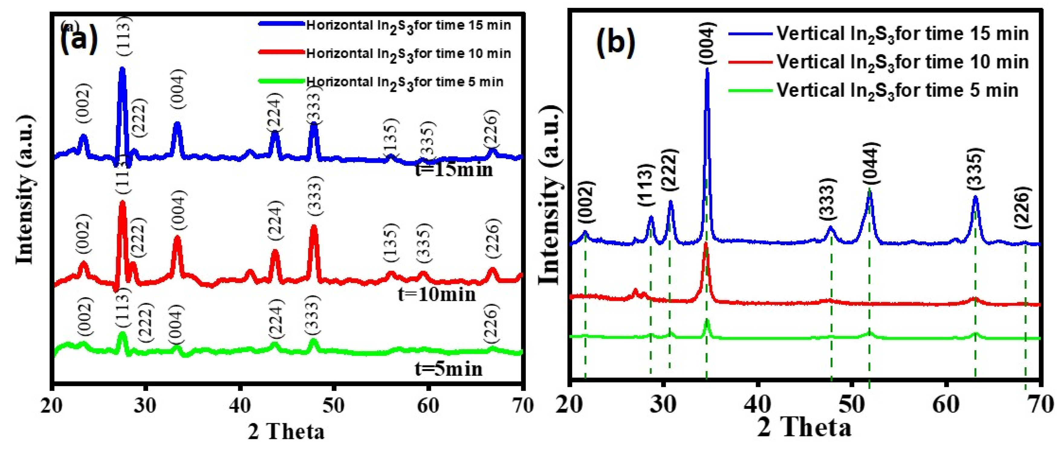
Structural and phase analysis was done by XRD and Raman analysis for vertical and horizontal gron In2S3 nanoflakes, which shows the formation of β-In2S3 [30]. Figure 1(a) and (b) shows the XRD graph of vertical and horizontal grown In2S3 nanoflakes. The existence of the tetragonal structure of β-In2S3 has been demonstrated by the maximum intensity peak at 27.52o with a hkl value of (113) in the XRD pattern of horizontal In2S3 nanoflakes while for vertical nanoflakes, the prominent peak was at 34.63o with hkl (004) plane. Further high-intensity peaks match the hkl values (002), (222), (004), (224), (333), (044), (135), (335) and (226) planes and are located at 23.52o, 28.78o, 33.35o, 43.74o, 47.76o, 50.38o, 56.31o, 59.67o, and 66.86o, respectively [31]. The peak at 34.63o shows the vertical growth of In2S3 nanosheets due to imperfect orientations in association with substrate. While high-intensity peaks in horizontal growth towards the lower 2θ range at 27.52o implies the layered growth due to the expansion of the Vanderwall gap.
Raman analysis is a strong technique to identify synthesized samples' thickness, phase, and chemical composition shown in Figure 2 [32]. Raman spectra for the sample prepared at the 550 oC and 750 oC growth temperature of with vertical and horizontal growth show the characteristic peaks for Eg mode at 268, F2g mode at 327 cm-1 Bg mode at 117 and 180 cm-1 and Ag mode at 248, 306, 370 cm-1 indicating the growth of pure tetragonal β-In2S3 phase. The ratio of F2g/Eg mode is 1.04 for vertical and 0.91 for horizontal growth, higher intensity for the F2g mode indicates a higher surface area and more scattering which implies vertical growth of the In2S3 nanoflakes and softening of Eg mode suggests that reduction in restoring force and enhancement in the Vanderwall forces which leads to horizontal growth of nanoflakes [33,34].

2.2. Morphological Analysis

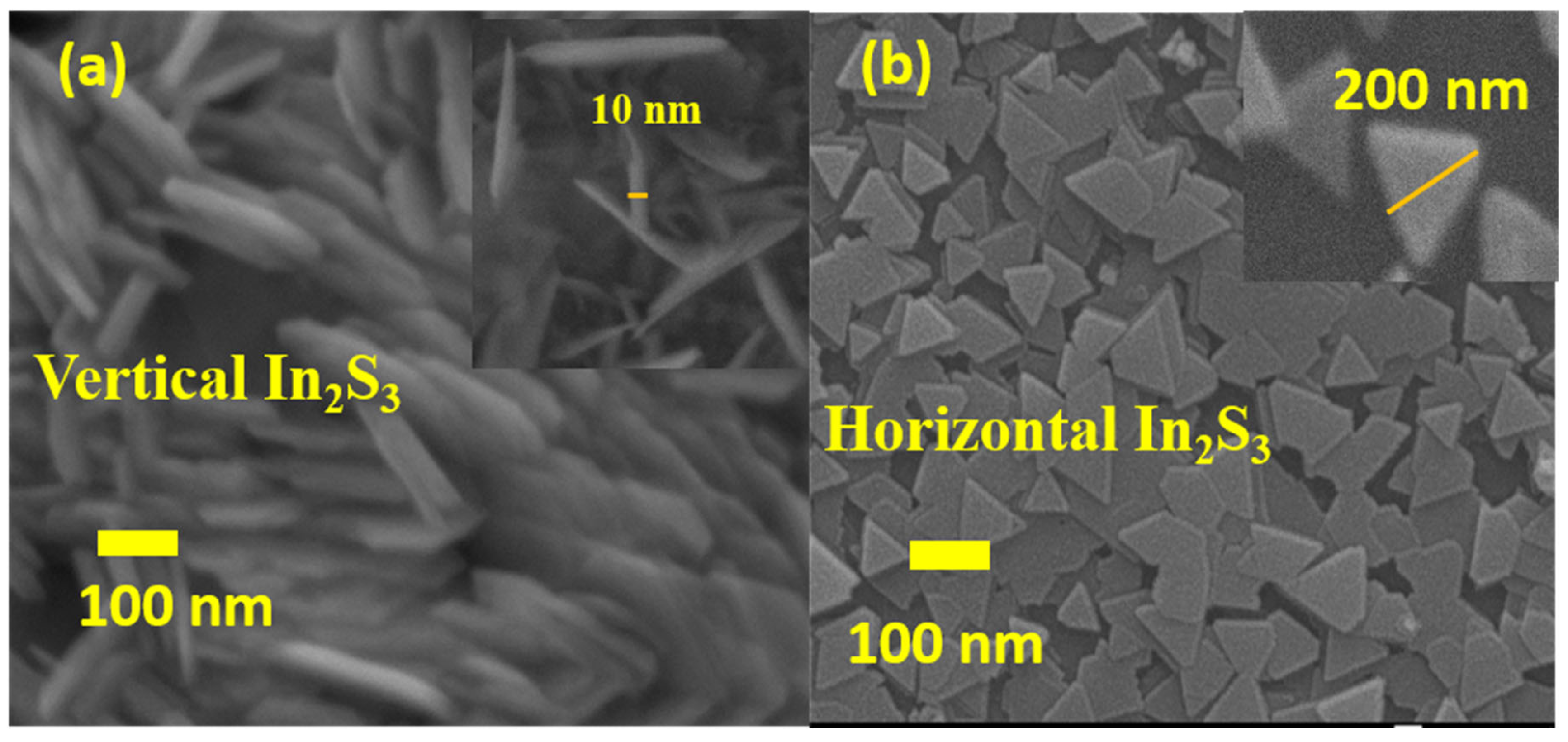
Morphology of different synthesized samples has been done by FESEM and AFM microscopy [35]. Figure 3 clearly shows the horizontal growth of In2S3 nanoflakes whereas Figure 3(a) shows the uniform vertical growth of In2S3 nanoflakes with the size of 10 nm and lateral thickness of 200 nm in Figure 3(b). It is seen that at the temperature of 550 oC vertical In2S3 nanoflakes have been formed and as the temperature goes on increasing horizontal nanoflakes start forming because initially, vertical seed growth has initiated because of less mobility, nucleation process dominates, while on increasing temperature film surface flattened and growth mechanism dominates results in horizontal nanoflakes [36].

2.3. XPS Analysis

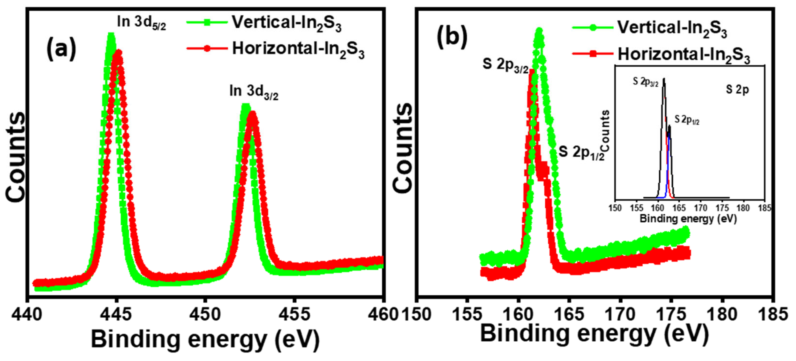
To analyze the valence state and chemical composition of the synthesized sample XPS analysis [37] has been shown in Figure 4(a and b). The High-resolution for In showing a 3+ state with peaks position at 444.8 eV and 452.4 eV which are indexed to In 3d5/2 and 3d3/2, whereas XPS spectra for Sulfur confirm S 2p3/2 and S 2p1/2 for binding energy value 161.5 eV and shoulder peak 162.7 eV respectively. For both vertical and horizontal samples there is a slight shift in the lower binding energy for In and S which is due to a change in the chemical environment of S due to the lateral and vertical growth of In2S3 nanoflakes [38].

2.4. Growth Mechanism of In2S3 Nanoflakes

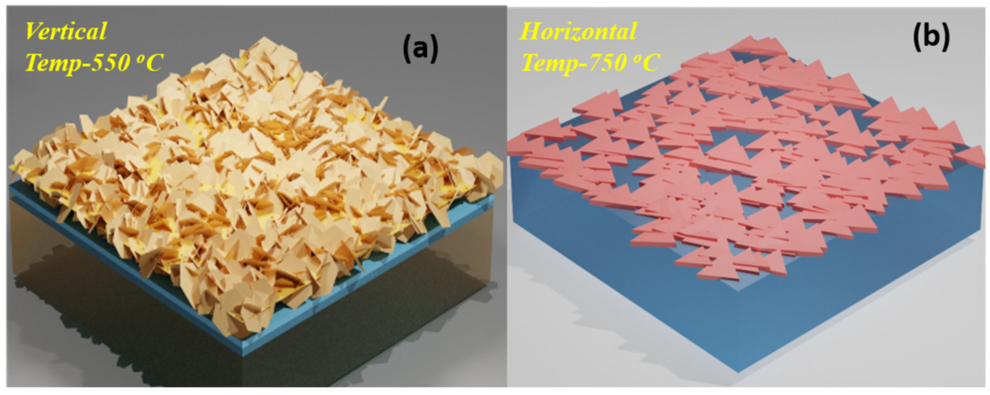
To generate TMDC layers with a regulated orientation and morphology, it is imperative to understand the growth mechanism. Previous research has demonstrated that the primary causes of the transition from horizontal to vertical growth are 1). Favored precursor adhesion at grain boundaries/defect sites 2).Squeezing and expulsion between the initial TMDC islands 3). Rapid sulphurization of the synthesized samples shown in Figure 5(a and b). These impacts will be explored concerning the evolution of growth behavior with deposition parameters. At low temperatures due to vertical seed growth and lesser expansion of the growth mechanism vertical nanoflakes were formed. In contrast, at a higher temperature, with higher adatom concentration, they are adsorbed back by the surface leading to lateral growth of In2S3 nanoflakes [39].

3. PEC Measurements

3.1. PEC Performance

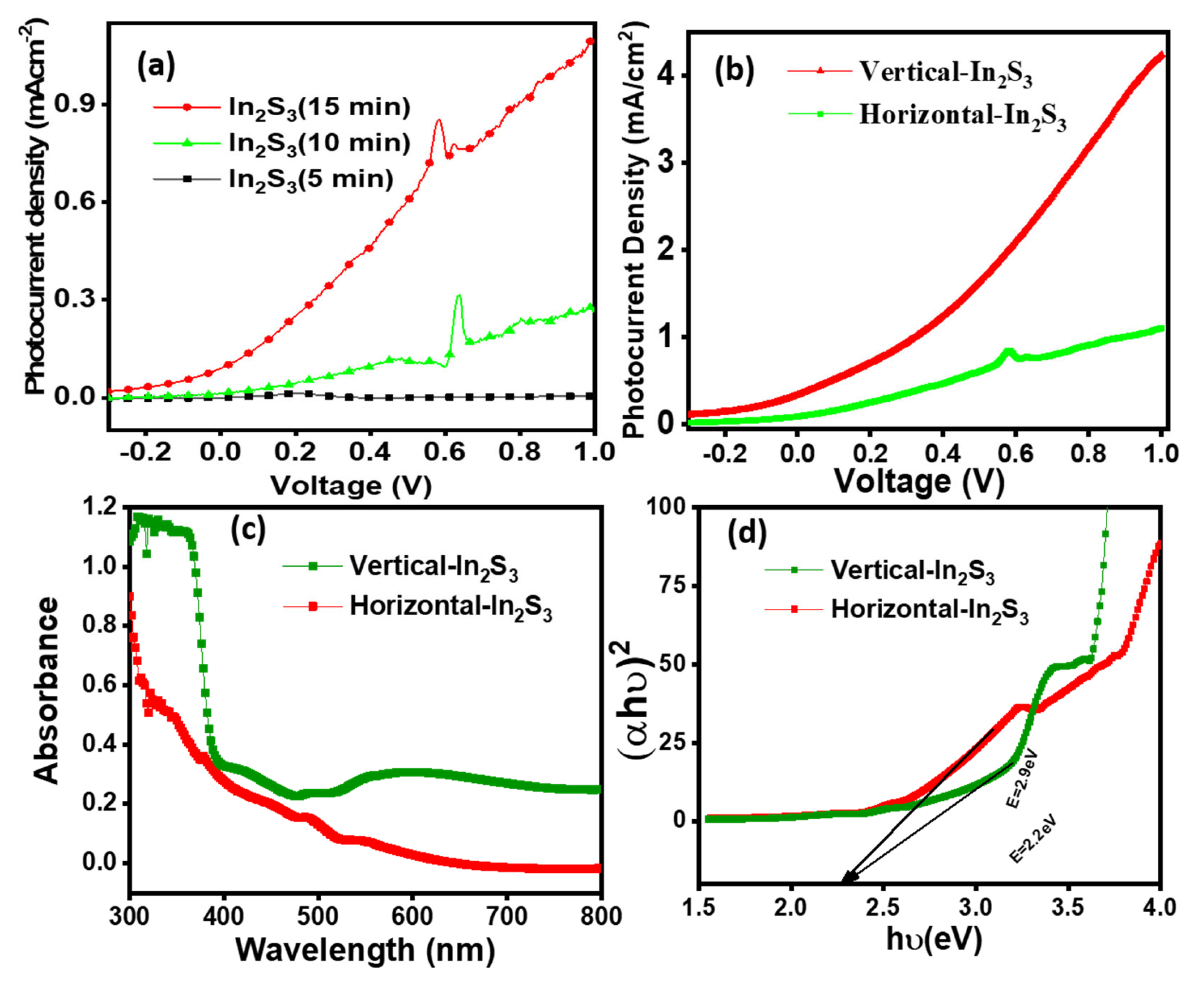
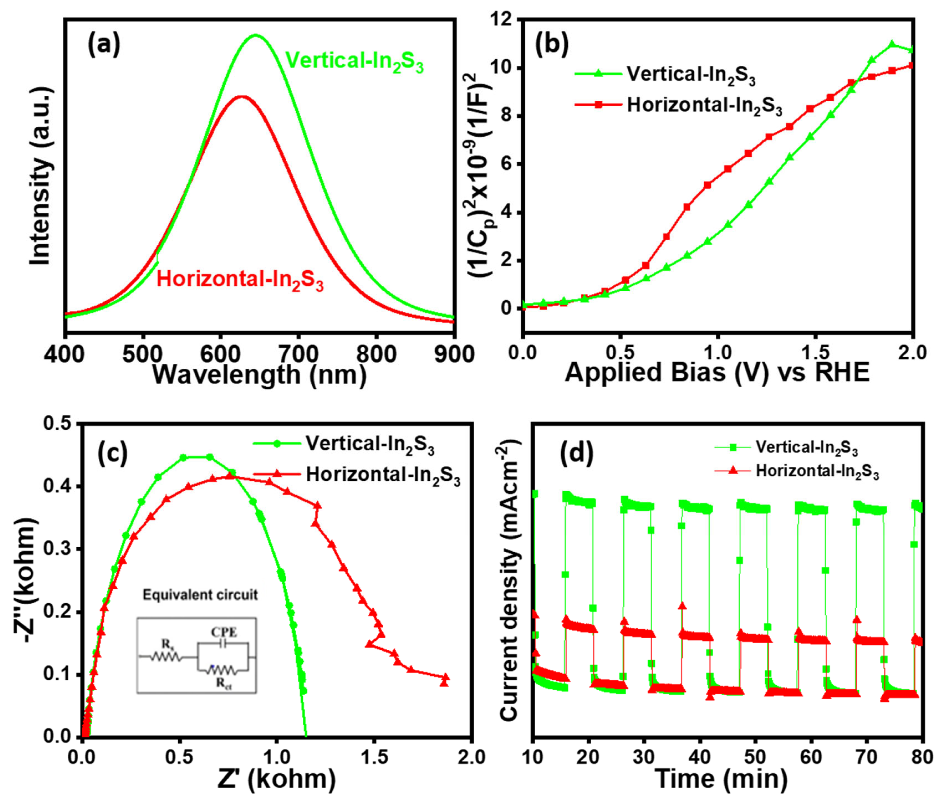
PEC measurements have been done for synthesized samples in both off and light conditions using 0.5 M Na2SO4 electrolyte [40]. It has been seen in Figure 6(and b) photocurrent density is 4.5 mAcm-2 for the vertical nanoflakes and 0.8 mAcm-2 for horizontal nanoflakes. This is because of more absorption shown in Figure 6(c), surface to volume ratio and due to enhancement in the vertical edge sites in the vertical nanoflakes than horizontal nanoflakes with bandgap value of 2.2 eV shown in Figure 6(d). This behavior is also attributed to Photoluminescence measurements which show that peaks for vertical and horizontal In2S3 nanoflakes show the maximum intensity at wavelength 600 nm which corresponds to its bandgap, while a slight shift towards longer wavelength for vertical In2S3 nanoflakes corresponds to more charge carriers at the interface and lesser recombination rate, which means lesser internal resistance to flow of charge carriers shown in Figure 7(a). Carrier density (ND) values and flat band potential (VFB) at vertical and horizontal In2S3 interface are calculated by the Mott-Schottky equation [40] at an applied frequency of 1 kHz.
1   C 2 = 2 q ϵ ϵ o N D V V F B k T q
where e is the electron charge, ϵo is the permittivity of vacuum [48] (ϵo= 8.85 x 10⁻¹⁴ Fcm-1), and ϵ is the dielectric constant which is 8.4 for In2S3 nanoflakes. a positive slope for both samples shows n-type conductivity in vertical and horizontal samples. Whereas flat band potential is 0.2 and 0.4 V for vertical and horizontal In2S3 nanoflakes respectively which also matches with on-set potentials for both samples shown in Figure 7 (b). The Carrier density (ND) value describes the number of photogenerated charges electrons and holes which is 6.7 x 1021 cm-3 and 2.2 x 1020 cm-3 for vertical and horizontal In2S3 respectively, which clearly show that high PEC performance for vertical In2S3 nanoflakes than horizontal In2S3 nanoflakes. To determine internal resistance to the flow of charge carriers Nyquist plot has been examined by determining the radius of the semicircle in the Z’ and Z” plot, which is smaller for vertical In2S3 nanoflakes than horizontal shown in the figure. This describes lower resistance to the flow of photogenerated charge carriers hence more photocurrent density for vertical nanoflakes. Internal resistance to flow of charge carriers is calculated by an equalvalent circuit and it is 1.9 kΩ for horizontal whereas it is 1.1 kΩ for vertical nanoflakes shown in Figure 7(c). Lesser resistance implies more flow of charge carriers and higher photocurrent density. Transient photocurrent density measurements were done with off and on conditions of light, which clearly show in Figure 7(d) the higher stability for the vertical nanoflakes than horizontal nanoflakes.

3.2. Quantitative Photoelectrochemical Measurement

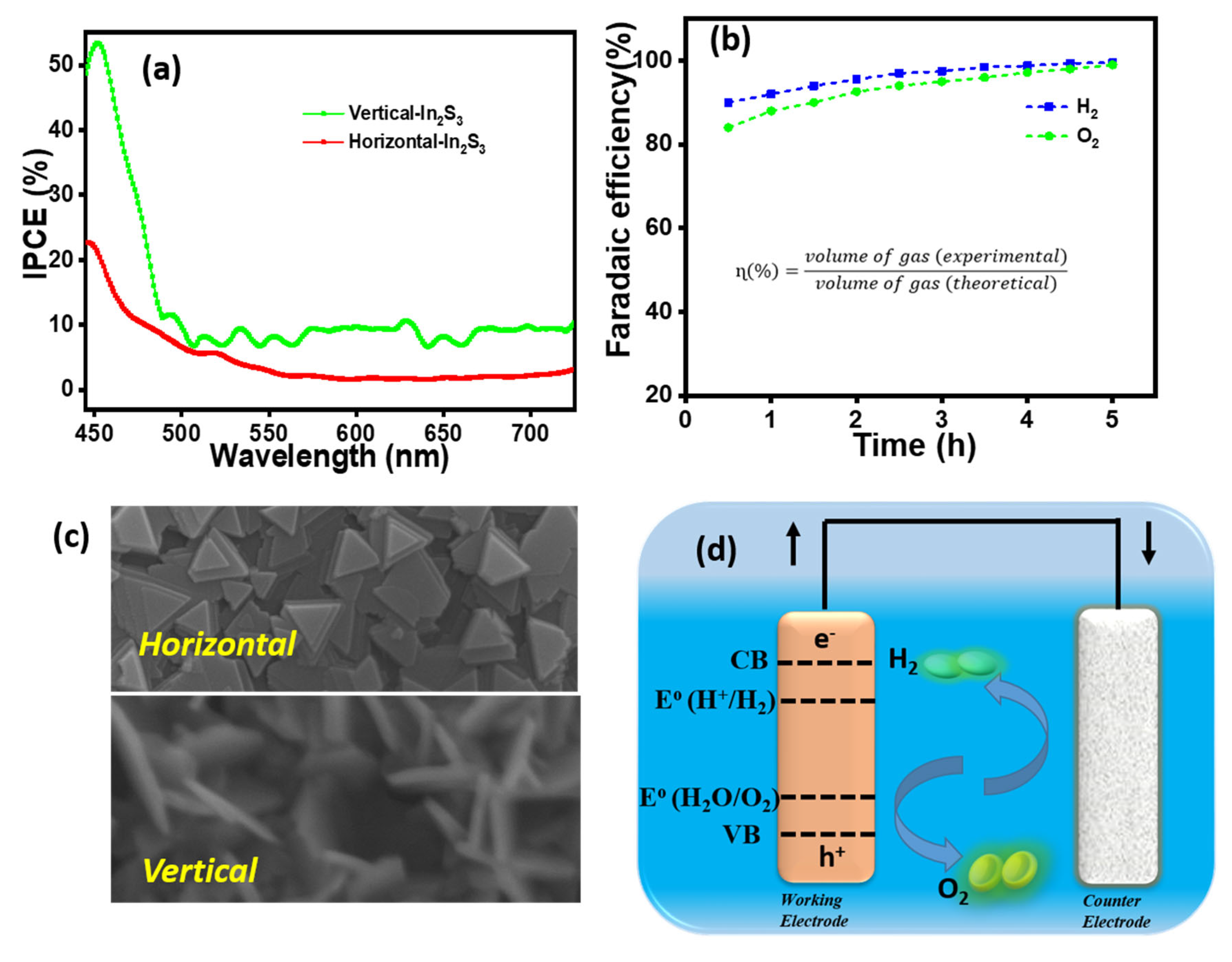
Quantitative PEC measurements were done from IPCE and faradic efficiency calculations. Figure 8(a) shows IPCE values for vertical In2S3 nanoflakes is 52% while 22% for horizontal nanoflakes, higher charge density calculations imply a lesser recombination rate of photogenerated charge carriers. Faradic efficeicy is also caluclted for vertical grown In2S3 nanoflkaes by equation [41].
ɳ % = v o l u m e   o f   g a s   e x p e r i m e n t a l v o l u m e   o f   g a s   t h e o r e t i c a l = v o l u m e   o f   g a s   e x p e r i m e n t a l R T I t p Z F
where R, T, I, t, p, Z, and F denotes ideal gas contact, the temperature of the gas, current, time, pressure, and the number of electrons for releasing one molecule, which is two for hydrogen and four for oxygen gas and the Faraday constant respectively. It is seen that Faradaic efficiency is 88 % and 90% for O2 and H2 respectively for the vertical In2S3 nanoflakes shown in Figure 8(b). Vertical nanoflakes are utilized in commercial PEC water splitting as their exist type energy band alignment shown in Figure 8(d). It has been seen that after PEC measuremnts in the electrolyte there is no effect on In2S3 samples which is clearly seen in Figure 8(c).

Conclusions

In this present study, orientation-controlled In2S3 nanoflakes were synthesized by the chemical vapor deposition technique by controlling temperature and growth time in the chemical vapor deposition technique. At lower temperatures due to the lesser energy of adatoms, seeding was done at the beginning which leads to the vertical growth of nanoflakes. Vertical-grown In2S3 nanoflakes have shown excellent photoelectrochemical response in terms of photocurrent density, IPCE efficiency, and faradic efficiency. This study leads to new insight into the growth of 2D In2S3 nanoflakes vertically and laterally.

Authors Contribution

Narinder Kaur Growth, characterize, conceptualization, investigation, writing of original and final draft, analysis of parameters.

Declaration of Competing Interest

The authors declare that they have no known competing financial interests or personal relationships that could have appeared to influence the work reported in this paper.

References

  1. Y. Li, C. Y. Xu, J. Y. Wang, and L. Zhen, Photodiode-like behavior and excellent photoresponse of vertical Si/monolayer MoS2 heterostructure, Scientific Reports, 2014, 4, 7186. [CrossRef]
  2. Zhenxing Wang Tofik Ahmed Shifa Yao Wen Fengmei Wang Xueying Zhan, Two-Dimensional Non-Layered Materials: Synthesis, Properties, and Applications, Adv fun materials,2016. [CrossRef]
  3. H. Xu, J. Wu, Q. Feng, N. Mao, C. Wang, and J. Zhang, High responsivity, and gate tunable graphene-MoS2 hybrid phototransistor, Nano Small 2014, 10, 2300.
  4. W.Haung, L. gang, H. Li, and T.Zhai, 2D Layered Group-IIIA Metal Chalcogenides: Synthesis, Properties and Applications in Electronics and Optoelectronics, RSC, 2016, 18, 22.
  5. Xiaobing Li, Jinzhan Su, Liejin Guo, vertically aligned ZnO/In2S3 core/shell heterostructures with enhanced photoelectrochemical properties, JMS,2020, pp. 15773-15784.
  6. Jih-Sheng Yang and Jih-Jen Wu, Toward Eco-Friendly and Highly Efficient Solar Water Splitting Using In2S3/Anatase/Rutile TiO2 Dual-Staggered-Heterojunction Nanodendrite Array Photoanode, ACS AMI, 2018, pp. 3714-3722.
  7. F. Liu, Y. Jiang, J.Yang, M.Hang, MoS2 nanodot decorated In2S3 nanoplates: a novel heterojunction with enhanced photoelectrochemical performance, RSC, 2016, 52, 1867.
  8. Narinder Kaur, Dipika Sharma, B.R. Mehta, Growth of In2S3 nanolayers on F-Mica, SiO2, ZnO, and TiO2 substrates using chemical vapor deposition, MSEB, 2021, pp. 114889-114897.
  9. Sudiksha Khadka, Thushan E. Wickramasinghe, Miles Lindquist, Ruhi Thorat, Shrouq H. Aleithan, Martin E. Kordesch, and Eric Stinaff, “ As grown tow dimensional MoS2 based photodetectors with naturally formed contacts”, Appl. Phys. Lett. 110, 261109 (2017); https://. [CrossRef]
  10. J. D. Yao, Z. Q. Zheng, J. M. Shao and G. W. Yang, “Stable, highly responsive and broadband photodetection based on large-area multi-layered WS2 films grown by pulsed-laser deposition, Nanoscale, 2015, 7, 14974-14981.
  11. Shouli Bai, Qiangqiang Li, Jingyi Han, Xiaojun Yang, Xin Shu, Jianhua Sun, Lixia Sun, Ruixian Luo, Dianqing Li, Aifan Chen, Photoanode of LDH catalyst decorated semiconductor heterojunction of BiVO4/CdS to enhance PEC water splitting efficiency, IJHE,2019, pp. 24642-24652.
  12. Xinglin Wen, Sijie Chen, Jiaxin Zhao, Wei Du, and Weijie Zhao, “Enhanced Plasmonic Hot-Carrier Transfer in Au/WS2 Heterojunctions under Nonequilibrium Condition”, ACS Photonics.
  13. J.Yu, Jie. Li, W. Zhang and H. Chang, Synthesis of high-quality two-dimensional materials via chemical vapor deposition, RSC, 2015, 6, 6705-6716.
  14. Haijin Li, Yuying Gao, Yong Zhou, Fengtao Fan, Qiutong Han, Qinfeng Xu, Xiaoyong Wang, Min Xiao, Can Li, and Zhigang Zou, Construction and Nanoscale Detection of Interfacial Charge Transfer of Elegant Z-Scheme WO3/Au/In2S3 Nanowire Arrays, Nano Letters, 2016, pp. 5547-5552.
  15. Narinder Kaur, Abhishek Ghosh, Mujeeb Ahmad, Dipika Sharma, Rajendra Singh, B.R. Mehta, “Increased visible light absorption and charge separation in 2 D–3 D In2S3- ZnO heterojunctions for enhanced photoelectrochemical water splitting, Jelcom, 903 (2022) 164007.
  16. Narinder Kaur, Abhishek Ghosh, Prashant Bisht, Arvind Kumar, Vishakha Kaushik, Nisha Kodan, Rajendra Singh and B.R.mehta, “Enhanced photodetection and a wider spectral range in the In2S3–ZnO 2D–3D heterojunction: combined optical absorption and enhanced carrier separation at the type-II heterojunction”, JMCC. [CrossRef]
  17. Aldona Jelinska, Krzysztof Bienkowski, Michal Jadwiszczak, Marcin Pisarek, Marcin Strawski, Dominik Kurzydlowski, Renata Solarska, and Jan Augustynski, “Enhanced Photocatalytic Water Splitting on Very Thin WO3 Films Activated by High-Temperature Annealing”, ACS Catalysis 2018 8 (11), 10573-10580.
  18. Yao, Y.; Sang, D.; Zou, L.; Wang, Q.; Liu, C. A Review on the Properties and Applications of WO3 Nanostructure-Based Optical and Electronic Devices. Nanomaterials 2021, 11, 2136. https://. [CrossRef]
  19. Y. Zhao, S. Balasubramanyam, R. Sinha, R. Lavrijsen, M. A. Verheijen, A. A. Bol, and A. Bieberle-Hütter, “Physical and Chemical Defects in WO3 Thin Films and Their Impact on Photoelectrochemical Water Splitting”, ACS AEM, 2018 1 (11), 5887-5895. [CrossRef]
  20. Yuriy Pihosh, Ivan Turkevych, Kazuma Mawatari, Tomohiro Asai, Takashi Hisatomi, Jin Uemura, Masahiro Tosa, Kiyoshi Shimamura, Jun Kubota, Kazunari Domen, and Takehiko Kitamori, “Nanostructured WO3/BiVO4 Photoanodes for Efficient Photoelectrochemical Water Splitting”, small 2014, 10, No. 18, 3692–3699.
  21. Narinder Kaur, Dipika Sharma, B.R. Mehta, “Growth of In2S3 nanolayers on F-Mica, SiO2, ZnO, and TiO2 substrates using chemical vapor deposition”, MSEB, Volume 264, 2021, 114889.
  22. Chang, Y., Wang, J., Wu, F., Tian, W. and Zhai, W., 2020. Structural Design and Pyroelectric Property of SnS/CdS Heterojunctions Contrived for Low-Temperature Visible Photodetectors. Adv Fun Materials, 30(23), p.2001450Hairui Liu, Haifa Zhai, Chunjie Hu, Jien Yang, and Zhiyong Liu, Hydrothermal synthesis of In2O3 nanoparticles hybrid twins hexagonal disk ZnO heterostructures for enhanced photocatalytic activities and stability, Nanoscale research latter, 2017, pp. 2183-2193.
  23. Michał Mazur, Damian Wojcieszak, Artur Wiatrowski, Danuta Kaczmarek, Aneta Lubańska, Jarosław Domaradzki, Piotr Mazur, Małgorzata Kalisz, “Analysis of amorphous tungsten oxide thin films deposited by magnetron sputtering for application in transparent electronics”, Applied Surface Science, Volume 570, 2021, 151151, ISSN 0169-4332. [CrossRef]
  24. Narinder Kaur, Dipika Sharma, B.R. Mehta, “Growth of specific geometries such as cubes of In2S3 for PEC water splitting by hydrothermal technique”, Materials Today: Proceedings 50, 7-10.
  25. Zhiwei Wang, Guang Yang, Chiew Kei Tan, Tam Duy Nguyen, Alfred Iing Yoong Tok, “Amorphous TiO2 coated hierarchical WO3 Nanosheet/CdS Nanorod arrays for improved photoelectrochemical performance”, Applied Surface Science 490 (2019) 411–419.
  26. Xiaobing Li, Jinzhan Su and Liejin Guo, Vertically aligned ZnO/In2S3 core/shell heterostructures with enhanced photoelectrochemical properties, Journal of Material Science: Materials in electronics, 2020, pp.15773-15784.
  27. Daniel Commandeur, Joshua McGuckin, Steven Firth, Rong Qian, and Qiao Chen, Goethite and Hematite Hybrid Nanosheet-Decorated YZnO NRs for Efficient Solar Water Splitting, JPCC, 2021, pp. 1673-1683.
  28. Chih-Hao Lu, Min Hsiung Hon, Chi-Yun Kuan, and Ing-Chi Leu, “Preparation of WO3 nanorods by a hydrothermal method for electrochromic device”, Japanese Journal of Applied Physics 53, 06JG08 (2014).
  29. Ming Li, X. Tu, Y.Su, J.Lu., Controlled growth of vertically aligned ultrathin In2S3 nanosheet arrays for photoelectrochemical water splitting, Nanoscale,2018,10,1153-1161.
  30. Song, W., Zhang, R., Bai, X. Exposed crystal facets of WO3 nanosheets by phase control on NO2-sensing performance. J Mater Sci: Mater Electron 31, 610–620 (2020).
  31. Hairui Liu, Haifa Zhai, Chunjie Hu, Jien Yang and Zhiyong Liu, Hydrothermal synthesis of In2O3 nanoparticles hybrid twins’ hexagonal disk ZnO heterostructures for enhanced photocatalytic activities and stability, Nanoscale Research Letters,2017, pp. 466-476.
  32. Young Bum Lee, Seong Ku Kim, Yi Rang Lim, In Su Jeon, Wooseok Song, Sung Myung, Sun Sook Lee, Jongsun Lim, and Ki-Seok An, “Dimensional-Hybrid Structures of 2D Materials with ZnO Nanostructures via pH-Mediated Hydrothermal Growth for Flexible UV Photodetectors”, ACS Appl. Mater. Interfaces 2017, 9, 15031−15037.
  33. B.Hemanth Kumar, S.Shaji, M.C.Santosh Kumar, Fabrication of visible light photodetector using co-evaporated Indium Sulfide thin films, JMS, 2019,30, 17986-17998.
  34. Cigdem Tuc Altaf, Nazire Simay Sahsuvar, Nazrin Abdullayeva, Ozlem Coskun, Alihan Kumtepe, Emine Karagoz, Mehmet Sankir, and Nurdan Demirci Sankir, Inverted Configuration of Cu (In, Ga)S2/In2S3 on 3D-ZnO/ZnSnO3 Bilayer System for Highly Efficient Photoelectrochemical Water Splitting, ASC Sustainable chemistry and engineering, 2020, pp. 15209-15222.
  35. Xiaoyang Feng, Yubin Chen, Zhixiao Qin, Menglong Wang, and Liejin Guo, “Facile Fabrication of Sandwich Structured WO3 Nanoplate Arrays for Efficient Photoelectrochemical Water Splitting” ACS AMI, 2016 8 (28), 18089-1809.
  36. Wenjuan Huang, Lin Gan, Haotian Yang, Nan Zhou, Renyan Wang, Wanhui Wu, Huiqiao Li, Ying Ma, Haibo Zeng, and Tianyou Zhai, Controlled Synthesis of Ultrathin 2D β-In2S3 with Broadband Photoresponse by Chemical Vapor Deposition, Adv. Funct. Mater. 2017, 1702448.
  37. Young Bum Lee, Seong Ku Kim, Yi Rang Lim, In Su Jeon, Wooseok Song, Sung Myung, Sun Sook Lee, Jongsun Lim, and Ki-Seok An, “Dimensional-Hybrid Structures of 2D Materials with ZnO Nanostructures via pH-Mediated Hydrothermal Growth for Flexible UV Photodetectors”, ACS Appl. Mater. Interfaces 2017, 9, 15031−15037.
  38. Monika Moun, R singh, 2019, “Study of the photoresponse behavior of a high barrier Pd/MoS2/Pd photodetector”, J. Phys. D: Appl. Phys. 52 325102.
  39. Ikram, M., Sajid, M.M., Javed, Y. Crystalline growth of tungsten trioxide (WO3) nanorods and their development as an electrochemical sensor for selective detection of vitamin C. J Mater Sci: Mater Electron 32, 6344–6357 (2021).
  40. Haijin Li, Yuying Gao, Yong Zhou, Fengtao Fan, Qiutong Han, Qinfeng Xu, Xiaoyong Wang, Min Xiao, Can Li, and Zhigang Zou, Construction and Nanoscale Detection of Interfacial Charge Transfer of Elegant Z-Scheme WO3/Au/In2S3 Nanowire Arrays, Nano Letters, 2016, pp. 5547-5552.
  41. Cigdem Tuc Altaf, Nazire Simay Sahsuvar, Nazrin Abdullayeva, Ozlem Coskun, Alihan Kumtepe, Emine Karagoz, Mehmet Sankir, and Nurdan Demirci Sankir, Inverted Configuration of Cu (In, Ga)S2/In2S3 on 3D-ZnO/ZnSnO3 Bilayer System for Highly Efficient Photoelectrochemical Water Splitting, ASC Sustainable chemistry and engineering, 2020, pp. 15209-15222.
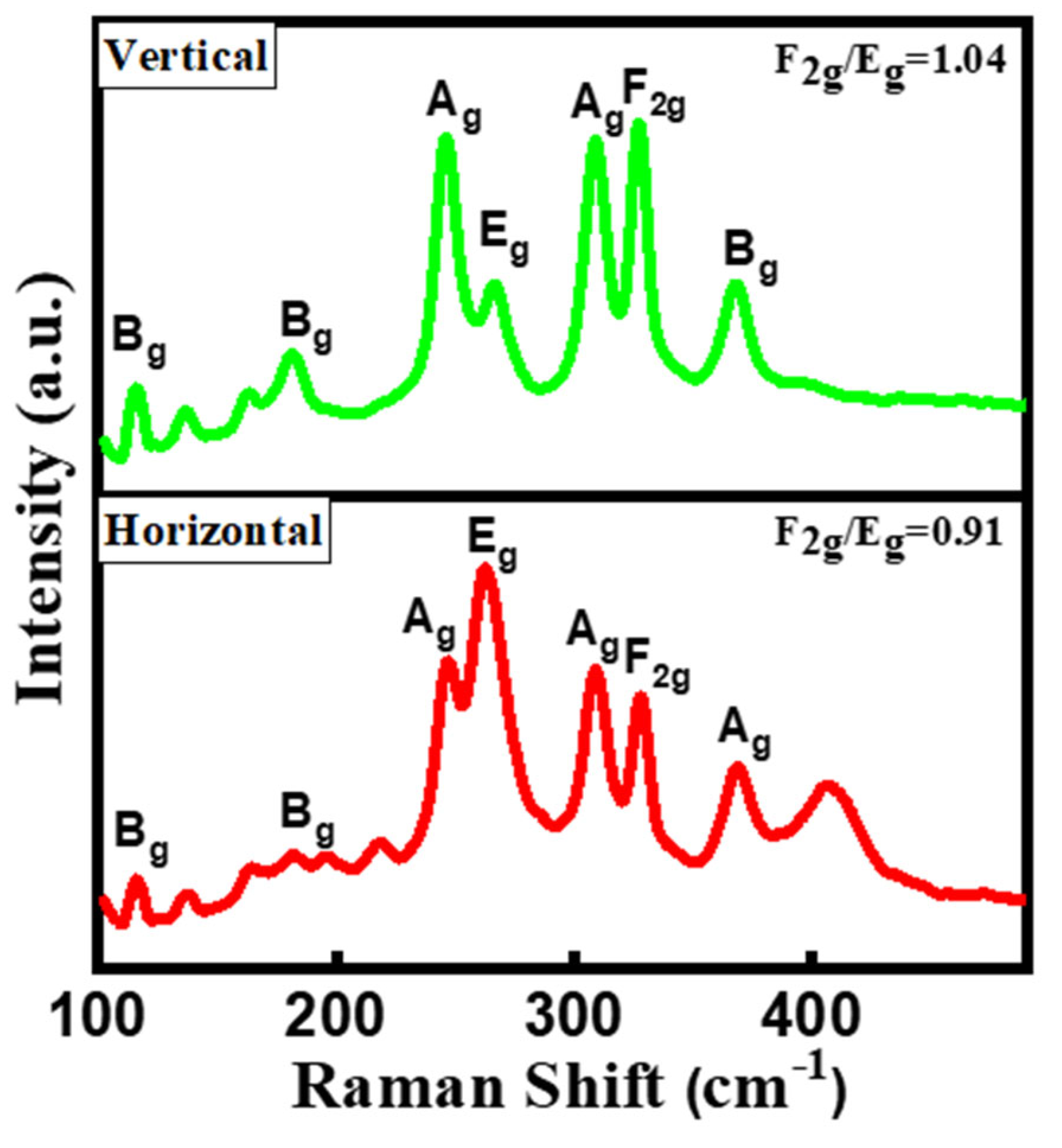
Figure 1. a) XRD graph for horizontal In2S3 nanoflakes (b) XRD graph for vertical In2S3 nanoflakes.
Preprints 120826 g001
Figure 2. Raman spectra for both vertical and horizontal In2S3 nanoflakes.
Preprints 120826 g002
Figure 3. (a) FESEM inset size measurement for Vertical In2S3 nanoflakes (b) FESEM inset size measurement for horizontal In2S3 nanoflakes.
Preprints 120826 g003
Figure 4. XPS spectra for (a) Indium and (b) Sulfur in both vertical and horizontal In2S3 nanoflakes.
Preprints 120826 g004
Figure 5. a) Vertical and (b) horizontal growth of In2S3 nanoflakes.
Preprints 120826 g005
Figure 6. (a),(b)Photocurrent density (c) Absorption plot (d) Tauc Plot for vertical and horizontal In2S3 nanoflakes.
Preprints 120826 g006
Figure 7. (a) Photolumnicense (b) Mott-Schottky plot (c) Nquist plot (d) Transient photocurrent density for vertical and horizontal In2S3 nanoflakes.
Preprints 120826 g007
Figure 8. a) IPCE measurements (b) Faradic efficiency (c) FESEM images after PEC test (d) Energy band diagram for vertical and horizontal In2S3 nanoflakes.
Preprints 120826 g008
Disclaimer/Publisher’s Note: The statements, opinions and data contained in all publications are solely those of the individual author(s) and contributor(s) and not of MDPI and/or the editor(s). MDPI and/or the editor(s) disclaim responsibility for any injury to people or property resulting from any ideas, methods, instructions or products referred to in the content.
Copyright: This open access article is published under a Creative Commons CC BY 4.0 license, which permit the free download, distribution, and reuse, provided that the author and preprint are cited in any reuse.
Prerpints.org logo

Preprints.org is a free preprint server supported by MDPI in Basel, Switzerland.

Subscribe

© 2024 MDPI (Basel, Switzerland) unless otherwise stated