Preprint
Article

Theoretical Study of Electron-Surface Optical Phonon Interaction in Monolayer Transition Metal Dichalcogenides Deposited on SiC and Hexagonal BN Dielectric Substrates in the Vicinity of the Points K+ K- of the Brillouin Zone

Altmetrics

Downloads

68

Views

119

Comments

0

A peer-reviewed article of this preprint also exists.

Submitted:

10 October 2024

Posted:

11 October 2024

You are already at the latest version

Alerts
Abstract
We investigated theoretically the electron-surface optical phonon interaction across the long-range Fröhlich coupling in monolayer transition metal dichalcogenides such as WS2, WSe2, MoS2, and MoSe2 monolayers on SiC and hexagonal BN dielectric substrates. We employed the effective Hamiltonian in the 〖K_(+ ) (K〗_-) valley of the hexagonal Brillouin zone, to assess electronic energy shifts induced by the interaction between electronic states and surface polar optical phonons. Our results indicate that the interaction between electron and surface optical phonon depends upon the polar nature of the substrate. We have also calculated the polaronic oscillator strength as well as the polaronic scattering rate of the lower polaron state in monolayer WS2, WSe2, MoS2, and MoSe2 on SiC and hexagonal BN dielectric substrates. As a result, we have proved theoretically; firstly, the enhancement of polaronic scattering rate with temperature, and secondly, the notable influence of the careful selection of surrounding dielectrics on both Polaronic oscillator strength and polaronic scattering rate. Thus, the optimal dielectrics would be those exhibiting both elevated optical phonon energy and a high static dielectric constant.
Keywords: 
Subject: Chemistry and Materials Science  -   Materials Science and Technology

1. Introduction

In the past few years, there has been a growing interest in Transition Metal Dichalcogenides (TMDCs), specifically in the form of monolayer (ML) van der Waals materials. This has sparked significant research interest for various applications in electronics and optoelectronics [1,2,3].
In comparison to conventional semiconductors, such as GaAs, the Coulomb interaction between conduction electrons and valence holes, as well as the oscillator strengths of excitons in MLs TMDCs, are significantly higher due to the two-dimensional confinement of charge carriers, heavy effective masses, and weak screening in 2D systems [4,5,6,7,8,9]. That is why scientists studying the physics of semiconductor nanosystems have been very interested in 2D materials during the past few years, such as graphene, hexagonal boron nitride MLs, TMDC MLs, and the heterostructures they generate [10,11]. The ML TDMCs that have been investigated the most are MoS2, MoSe2, WS2, and WSe2 [12,13].
The transport of carriers in ML 2D materials under low fields is influenced by multiple scattering mechanisms, including interactions with acoustic and optical phonons. Additionally, scattering can occur due to polar coupling with the substrate beneath or with dielectrics, introducing another factor involving remote optical phonons. Thus, Polar optical phonons, situated at the interface, play a significant role in scattering carriers in TMDCs through the Fröhlich coupling. [14,15,16,17]. Therefore, it is crucial to comprehend these scattering events by examining the coupling between surface optical phonons (SOP) and electrons in TMDCs. Developing models that can elucidate experimental results becomes essential. This coupling is typically characterized by interactions between electronic excitations and phonons, giving rise to various intriguing effects in a crystal, including the formation of polarons [14,15,16,17,18,19,20].
Several studies in the literature proved the importance of the role played by the SOP coupling in the optical proprieties in ML TDMCs deposited on polar substrates. As an example, we referenced Suvodeep Paul et al. [21], who showed that the creation of a W S 2 h B N heterostructure leads to the coupling between electrons in W S 2 and polar phonons in h B N . This coupling governs the enhancement of defect-bound excitons and biexcitons. Additionally, they have performed an extensive resonant Raman analysis, varying both polarization and magnetic field, which provided further confirmation of the electron-phonon coupling in the W S 2 h B N heterostructure.
Likewise, Colin M. Chow et al. [22], observed a resonant Raman scattering phenomenon through cross-material exciton-phonon coupling at van der Waals interfaces. They noted that the sensitivity of excitons in monolayer materials to their phononic environments, such as those provided by S i O 2   , h B N , and sapphire, can be exploited to deepen our understanding of atomically thin devices. Else, Bastian Miller et al. [23], investigated exciton-phonon coupling in charge-tunable single-layer MoS2 devices using polarization-resolved Raman spectroscopy. They found a strong defect-mediated coupling between the long-range oscillating electric field of the longitudinal optical phonon in the dipolar medium and the exciton.
Sanjay Gopalan et al. [24] also explored the impact of the dielectric environment on electronic transport in monolayers TMDCs. By employing ab initio methods, they calculated the low-field carrier mobility in free-standing layers, considering the effects of dielectric screening on electron-phonon interactions induced by the bottom oxide and gate insulator, as well as scattering from hybrid interface optical-phonon/plasmon excitations. Their findings revealed that using insulators with a high dielectric constant can greatly improve carrier mobility.
This paper is structured as follows: first, we theoretically investigate the interaction between electrons and surface optical phonons in ML TMDCs on polar substrates, such as silicon carbide ( S i C ) and hexagonal boron nitride ( h B N ). Furthermore, we present a theoretical examination of the polaronic oscillator strength in ML TMDCs on polar substrates. Finally, we investigate the temperature dependence of the polaronic scattering rate in ML TDMCs on S i C and h B N polar substrates.

2. Electron-Surface Optical Phonon Interaction in ML TMDCs on S i C and h B N Dielectric Substrates

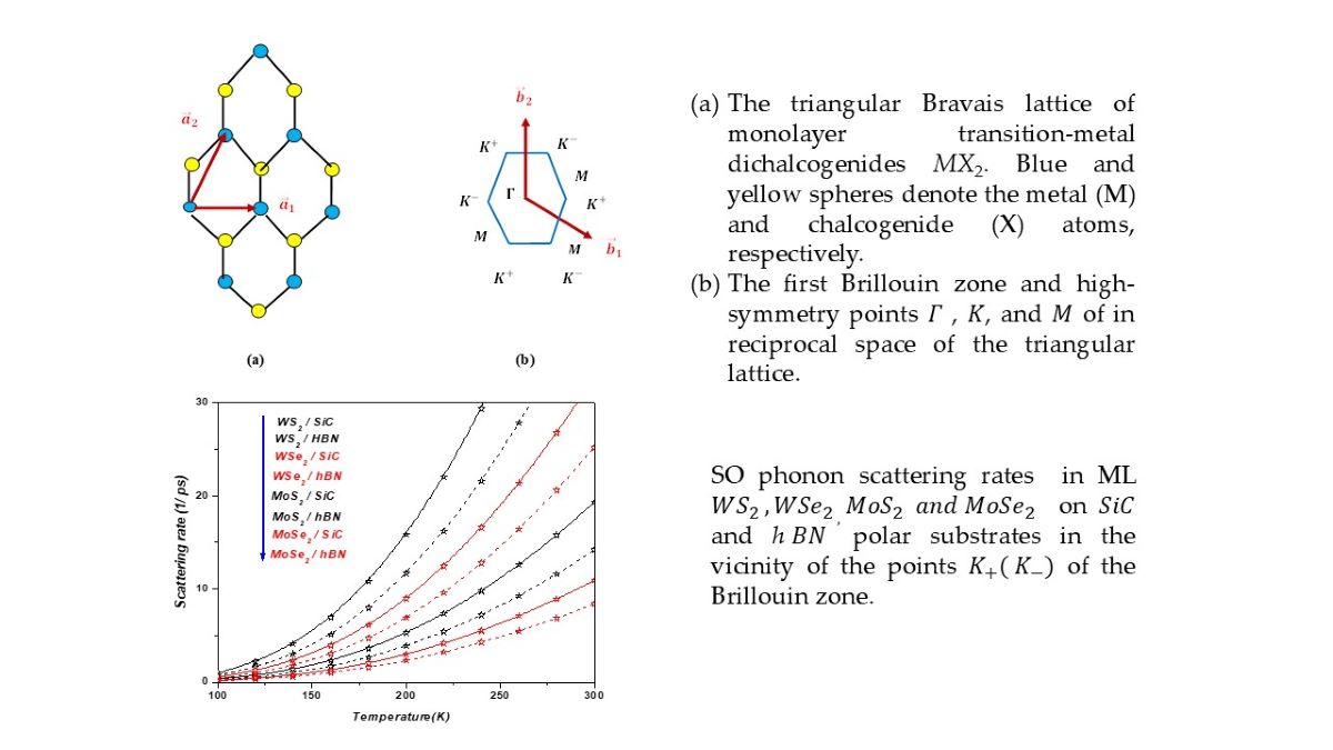
A monolayer transition metal dichalcogenide (TMDC) consists of a central layer of metal M atoms arranged in a triangular lattice, flanked by two layers of chalcogen X atoms positioned on the same triangular lattice. The triangular Bravais lattice is defined by the basis vectors:
a 1 = a 0 1 , 0,0 and a 2 = a 0 2 1 , 3 , 0 (see Figure 1a).
Figure 1b illustrates the reciprocal lattice, defined in relation to the triangular Bravais lattice and characterized by the vectors:
b 1 = 4 π 3 a 0 3 2 , 1 2 , 0 and b 2 = 4 π 3 a 0 0 , 1 , 0 where a 0 is the lattice constant.
The two-dimensional Brillouin zone of the TMDCs exhibits a hexagonal shape, featuring high-symmetry points denoted as Γ ,   K ,   a n d   M , each defined as follows:
Γ = 0 , 0 , K = 4 π 3 a 0 1 , 0 , M = 4 π 3 a 0 0 , 3 2
The effective 2×2 Hamiltonian characterizing the states of the conduction and valence bands with the parallel spins s = + 1 2 in the vicinity of the point K + is represented by the following expression [25,26,27]:
H + = E g 2 γ k x i k y γ k x + i k y E g 2  (1)
Where,   k = k x ,   k y denotes the two-dimensional wave vector of the electron measured from the point K + , the parameter γ is directly proportional to the interband matrix element of the momentum operator, γ = P 2 m * where m * is the electron effective mass and E g represents the width of the band gap.
The Hamiltonian describing a pair of spin sublevels with s = 1 2 in the same valley has the form of Equation (1) through the substitution E g E g + , where represents the sum of the spin–orbit splittings of the conduction and valence bands. The effective Hamiltonian in the K , valley is derived from Equation (1) through the substitution k x ± i k y k x i k y .
The energy spectrum of the electron derived from the Hamiltonian in Equation (1) has the Dirac form:
ε λ , k = λ ε k = E g 2 2 + γ 2 k 2  (2)
Here, λ = + and λ = correspond to the conduction and valence bands, respectively.
In our study, we use the assumption of homogeneous and defect-free interfaces between transition metal dichalcogenide monolayers and dielectric substrates as a simplification often used in theoretical models and simulations to make the problem tractable.
In this work we have investigated the electron surface optical phonon (SOP) interaction in ML TDMCs on S i C and h e x a g o n a l   B N dielectric substrates across the long-range Fröhlich coupling. Indeed, the long-range Fröhlich coupling model provides a robust framework for understanding electron-SOP interactions in TMDCs on polar substrates. However, it relies on several approximations; like for example Born-Oppenheimer Approximation [28]. Short-range interactions [29] (e.g., electron-phonon interactions in non-polar materials) are not considered. It assumes a constant effective mass for the electron, non-linear interactions and multi-phonon processes are typically neglected [30]. Impurities, defects, and other forms of disorder that can affect the electron-phonon interaction in real materials are usually not included in the idealized Fröhlich model [28,31]. The phonon dispersion is typically assumed to be linear, which is an approximation that might not hold for all phonon modes or substrates [32]. Often, a single dominant phonon mode is considered, neglecting the possible contribution of multiple phonon modes [29].
To simplify, our analysis, we consider the phonon spectrum as isotropic, implying that phonons exhibit either longitudinal or transverse polarization. The Fröhlich Hamiltonian introduces an interaction term wherein an electron scatters from k to k ' = k + q involving the emission or absorption of a phonon. In both cases the total momentum is conserved and is expressed as follows:
H = H p h + H e p h  (3)
The term   H p h denotes the phonon energies, incorporating both the Longitudinal Optical (LO) and Surface Optical (SO) modes, and can be expressed as:
H p h = q , ν ω ν a q + a q  (4)
In this context,   a q + , a q represent the creation and annihilation operators, respectively, for the phonon characterized by the wave vector q , while ω ν refers to the frequency of the phonon.
The second term H e p h is the Hamiltonian of interaction between electron and phonon [33]:
H e p h = q , ν M q , ν a q + + a q e i q r  (5)
The Fröhlich Hamiltonian is given as follow:
H = q , ν ω ν a q + a q + q , ν M q , ν a q + + a q e i q r (6)
The interaction between carriers in monolayer Transition Metal Dichalcogenides (TMDCs) and surface optical phonons is described by the second term in Equation (6).
The coupling element in the Fröhlich Hamiltonian M q ,   ν represents the interaction between the electron in TMDCs and surface optical phonon of the polar substrates. This matrix element is expressed as [34,35,36]:
V S O P = M q , S O = k k + q e 2 F ν 2 2 N A q e q z 0  (7)
In the given context, F ν 2 represents the magnitude of the polarization field, which is determined by the Fröhlich coupling [37]:
F ν 2 = ħ ω S O , ν 2 π 1 ε + ε e n v 1 ε 0 + ε e n v  (8)
While   ε 0   and ε   are the low- and high-frequency dielectric constants of the polar substrate, (refer to Table 1), z 0 represents the internal distance between the TMDCs and polar substrate (refer to Table 2). The term ħ ω S O , ν denotes the energy of SO phonon of the polar substrates with two branches ν = 1 ,   2 .
The SOP energies are extracted from the bulk longitudinal optical (LO) phonons as follows [38]:
ħ ω S O = ħ ω L O 1 + 1 ε 0 1 + 1 ε 1 2  (9
The screening of the Coulomb interaction by the polar dielectric environment is considered through   ε e n v . Given the weak screening of the electric field perpendicular to the plane of the ML TMDCs,   ε e n v   is set to1 [44].
On polar substrates, surface optical phonons (SOP) induce an electric field that interacts with the electrons in the neighboring ML TMDCs. Using Equations (7) and (8), the SOP coupling is expressed as:
W = q ψ k V S O P ψ k + q 2 = N A 2 π 2 1 cos θ k θ k + q 2 4 π 2 e 2 F ν 2 N A q e 2 q z 0 q d q d θ q  (10)
The summation is performed over one spin and one valley, where A = 3   2 a 2 is the area of the two-atom unit cell.
In our analysis in the present case, we have followed the same theoretical method presented in our previous calculations [14,15,16]. So, to study the interactions between electron and surface optical phonons in the ML TMDCs, we have specifically considered the electronic states ψ k   and ψ k + q   , with electron energies E k = ε k and E k + q = ε k + q , respectively. We have also considered the effective 2×2 Hamiltonian characterizing the states of the conduction and valence bands with the parallel spins s = ± 1 2 in the vicinity of the point K + ( K )   of the hexagonal Brillouin zone.
The space of polaronic states results from a tensor product between the two subspaces of electronic and phononic states. Thus, we consider new states called polaronic states given by:
ψ k + q , 0 q , ψ k , 1 q  (11)
The Polaron electron energies E ± e for the states ψ ± in ML TMDCs on polar substrates are given bellow [14,15,16]:
E ± e = 1 2 E k + q + E k + ω L O ± 1 2 E k + q E k + ω L O 2 + N A 2 π 2 1 cos θ k θ q 2 4 π 2 e 2 F ν 2 N A q e 2 q z 0 q d q d θ q  (12)
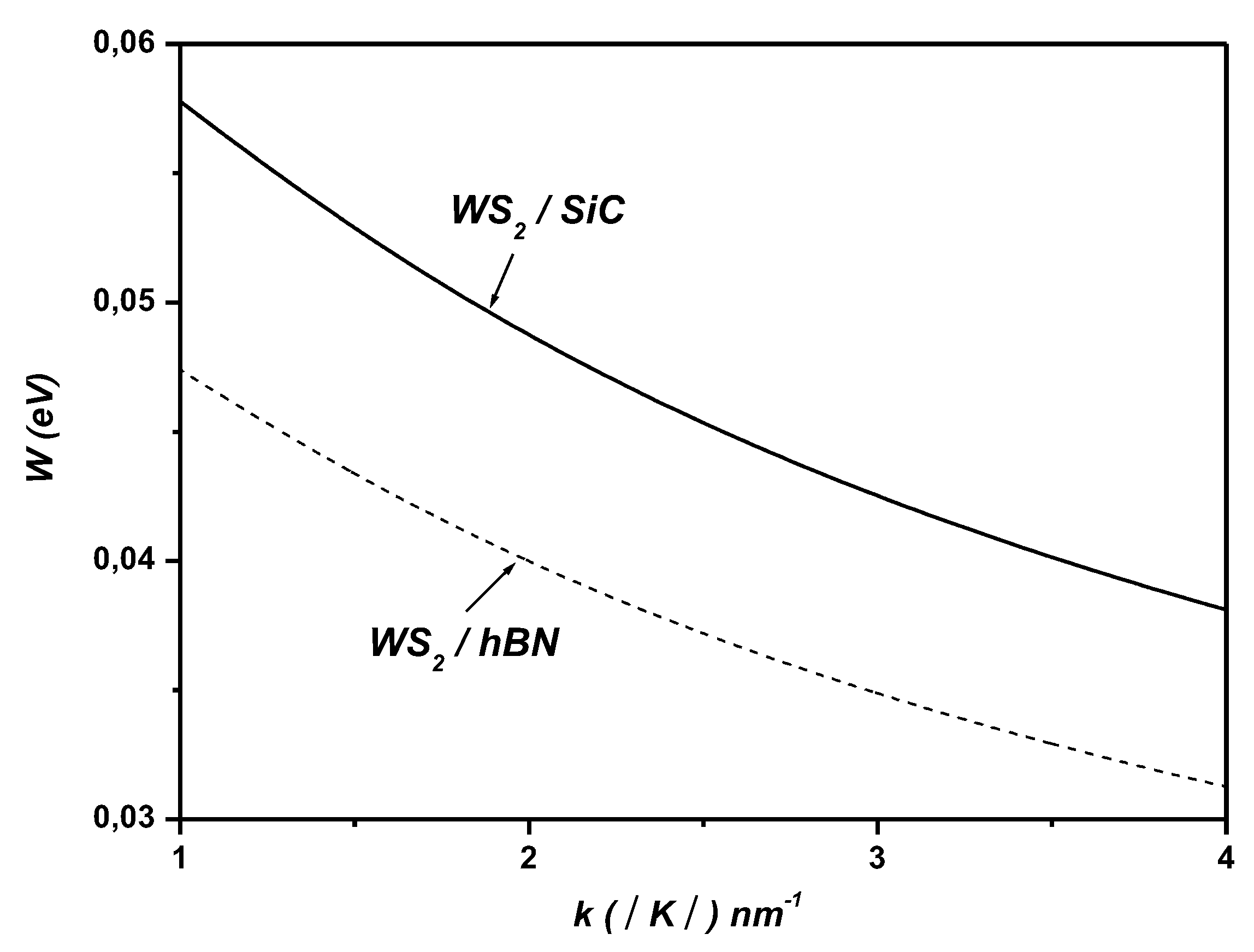
Figure 2 depicts the SO coupling strength between the electronic states ψ k   and ψ k + q   versus the wave vector k   in ML WS2 on S i C and h B N polar substrate. As shown in Figure 2, it is evident that the coupling with SOP is significantly influenced by the type of polar substrate.
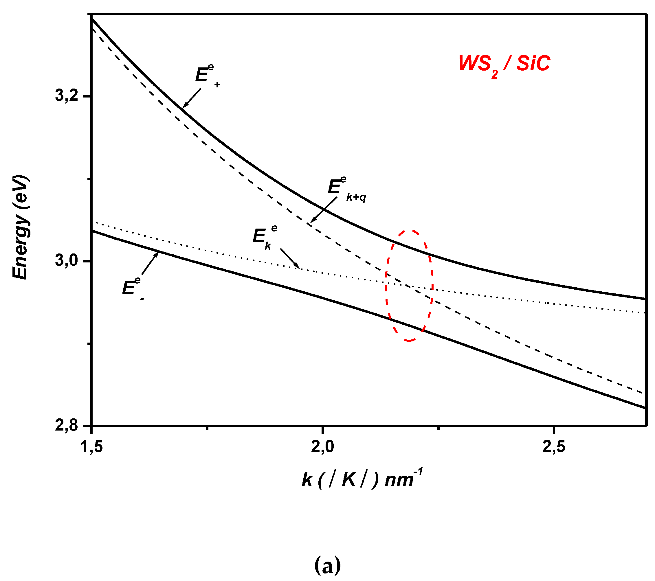
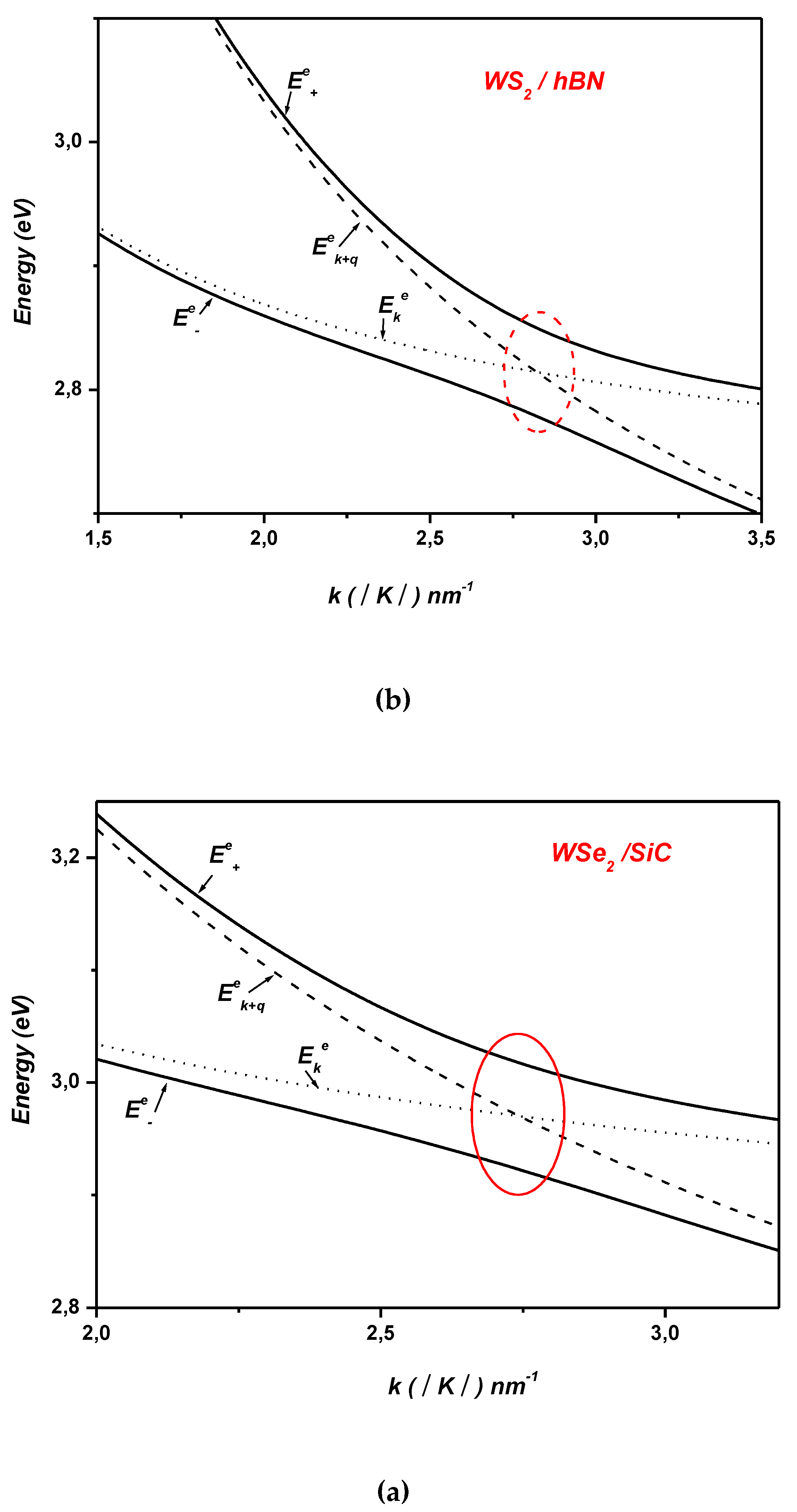
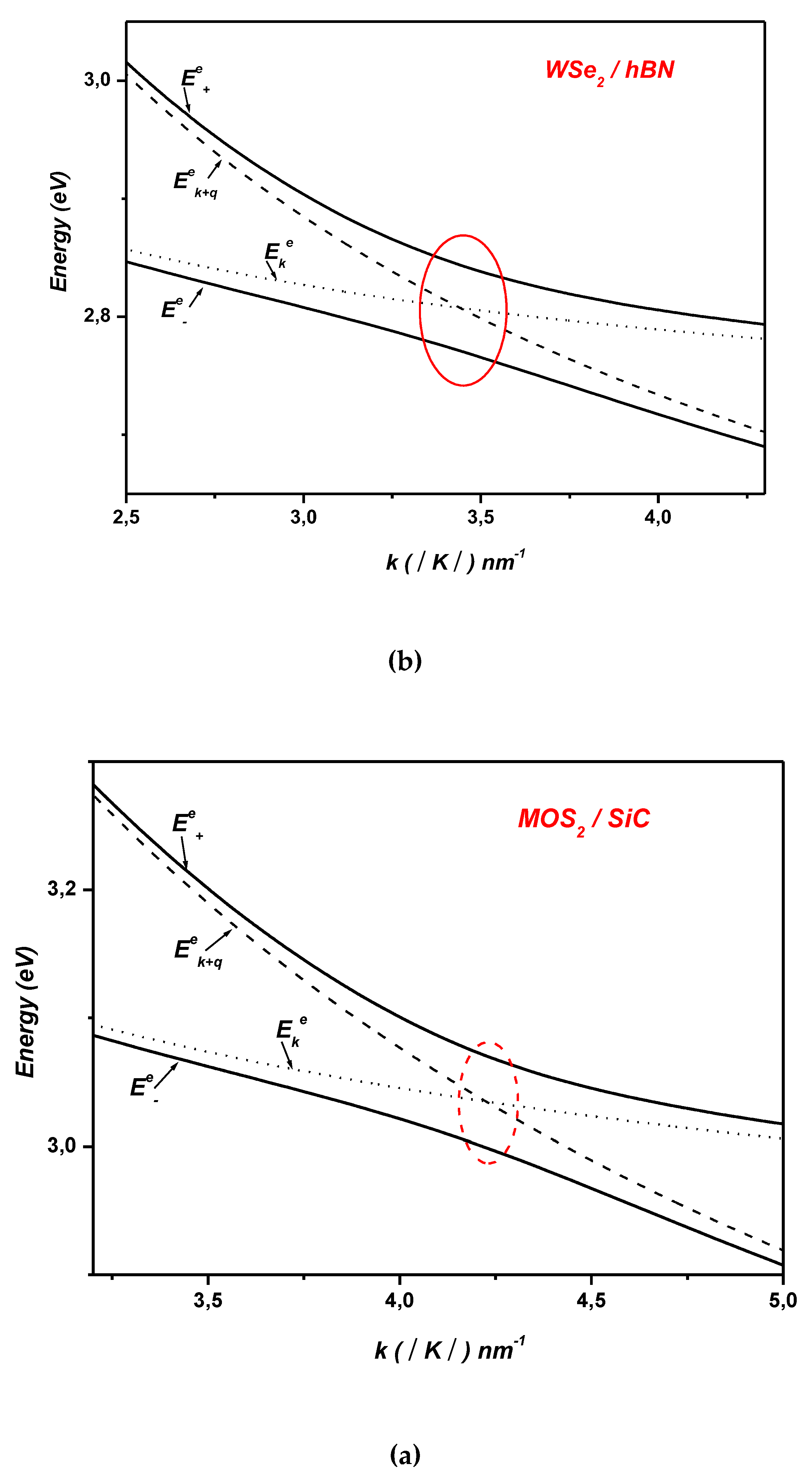
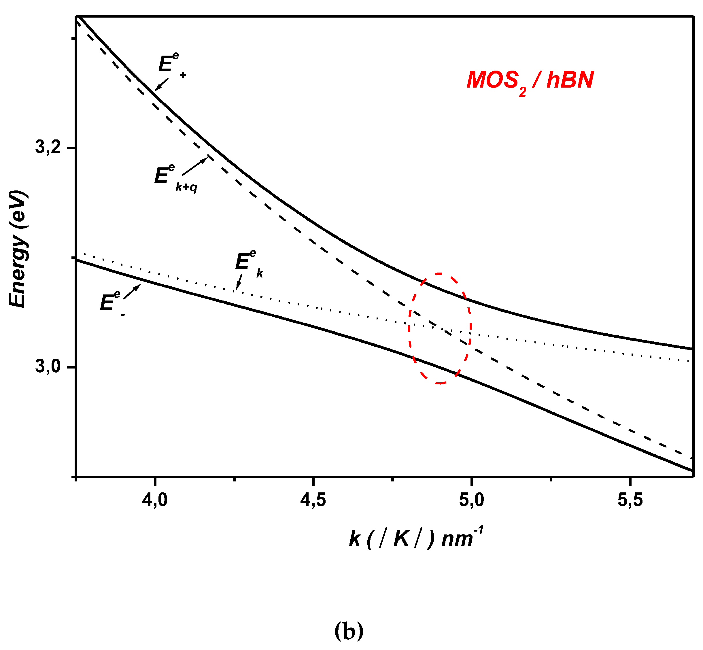
We show in Figure 3, the Polaron electron energies versus the wave vector k   in ML W S 2   ,   W S e 2   ,   M o S 2   a n d   M o S e 2 on S i C and h B N polar substrate. For comparison purposes, we have included in the same figures the energies of the non-interacting states ψ k + q   ,   0 q   and ψ k   ,   1 q . For example, in the case of WS2 these noninteracting levels cross near k ~ 2.2   n m 1 in the case of S i C and near k ~ 2.85 n m 1 in the case of h B N indicating resonant coupling (see Table 3). These crossings indicate that the separation between electronic levels is equal to ω L O for both S i C and h B N cases, where ω L O = 123.2   m e V   a n d   ω L O = 103.7   m e v respectively. In fact, the electronic level crossings are clearly replaced by significant anticrossings with energy levels approximately at ~94 meV and ~70 meV for S i C and h B N   polar substrates, respectively. It can be also observed in Figure 3, the enhancement of the Rabi splitting of the electron levels when shifting from h B N to S i C (refer Table 4).
In these anticrossings, the wave functions of the levels become mixed, allowing for multiple transitions such as E k E ± e   , E k E k + ω L O and E k E k + q . This demonstrates that the interaction between electrons and surface polar phonons cannot be considered a weak coupling. The coupling between electrons and SOP leads to the Rabi splitting of the electron levels. Hence, the calculations indicate the possibility of energetically resonant coupling between the electronic sub-levels and surface vibration modes in ML TMDCs on the studied polar substrates. Furthermore, the two resulting polaron states can be expressed as:
ψ ± = α ± ψ k + q , 0 q + β ± ψ k , 1 q (13)
The weight of electronic component   α ± and the weight of the one-phonon component β ± of the polaron states ± vary with the polaron energies E ± e . The expressions detailing these dependencies are as follows [14,15,16]:
α ± 2 = E ± e ω L O 2 E ± e ω L O 2 + N A 2 π 2 1 cos θ k θ k + q 2 4 π 2 e 2 F ν 2 N A q e 2 q z 0 q d q d θ q  (14)
β ± 2 = N A 2 π 2 1 cos θ q 2 4 π 2 e 2 F ν 2 N A q e 2 q z 0 q d q d θ q E ± e ω L O 2 + N A 2 π 2 1 cos θ k θ k + q 2 4 π 2 e 2 F ν 2 N A q e 2 q z 0 q d q d θ q  (15)
where N A 2 π 2 1 cos θ k θ k + q 2 4 π 2 e 2 F ν 2 N A q e 2 q z 0 q d q d θ q is the SO coupling strength between the electronic states ψ k   ,   1 q   a n d   ψ k + q   ,   0 q   [14,15,16,17].
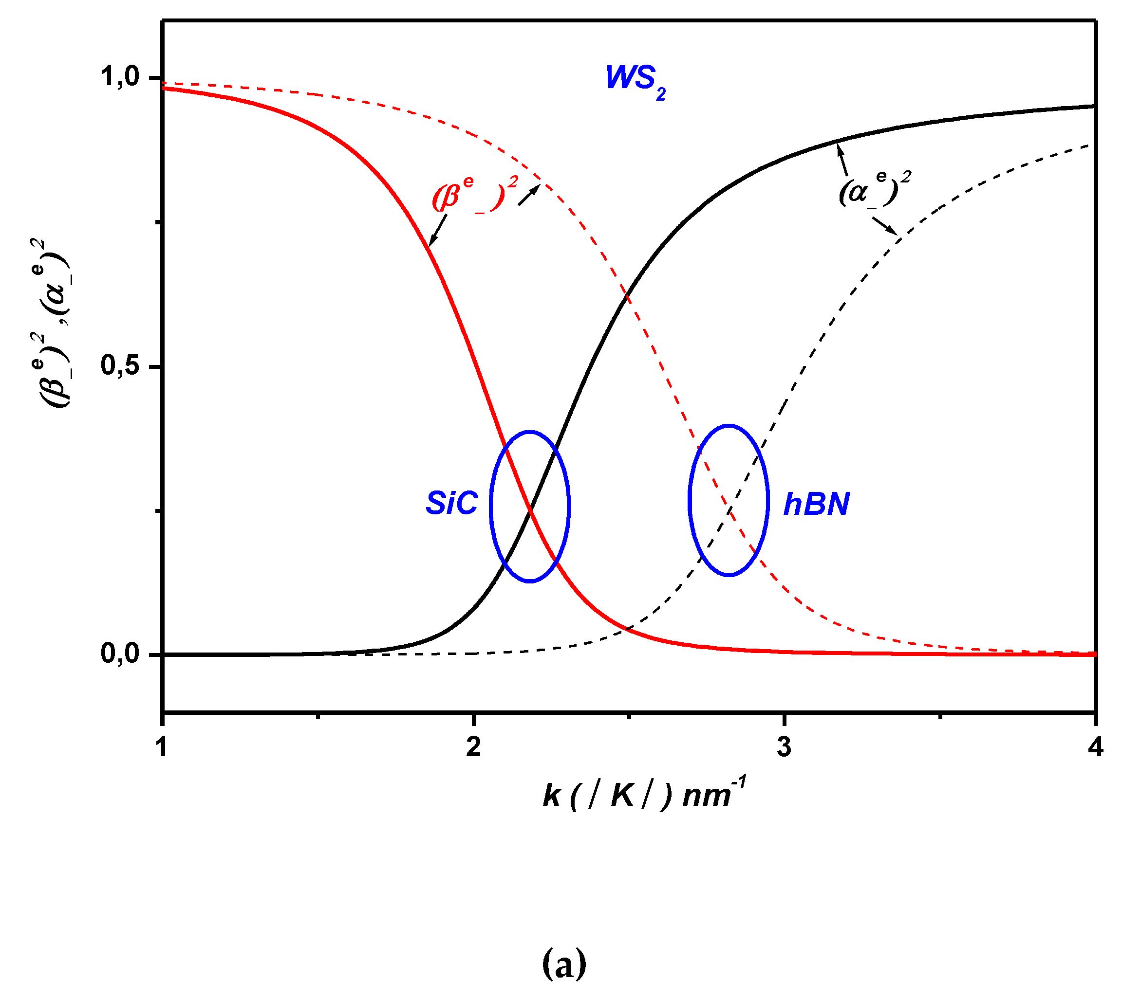
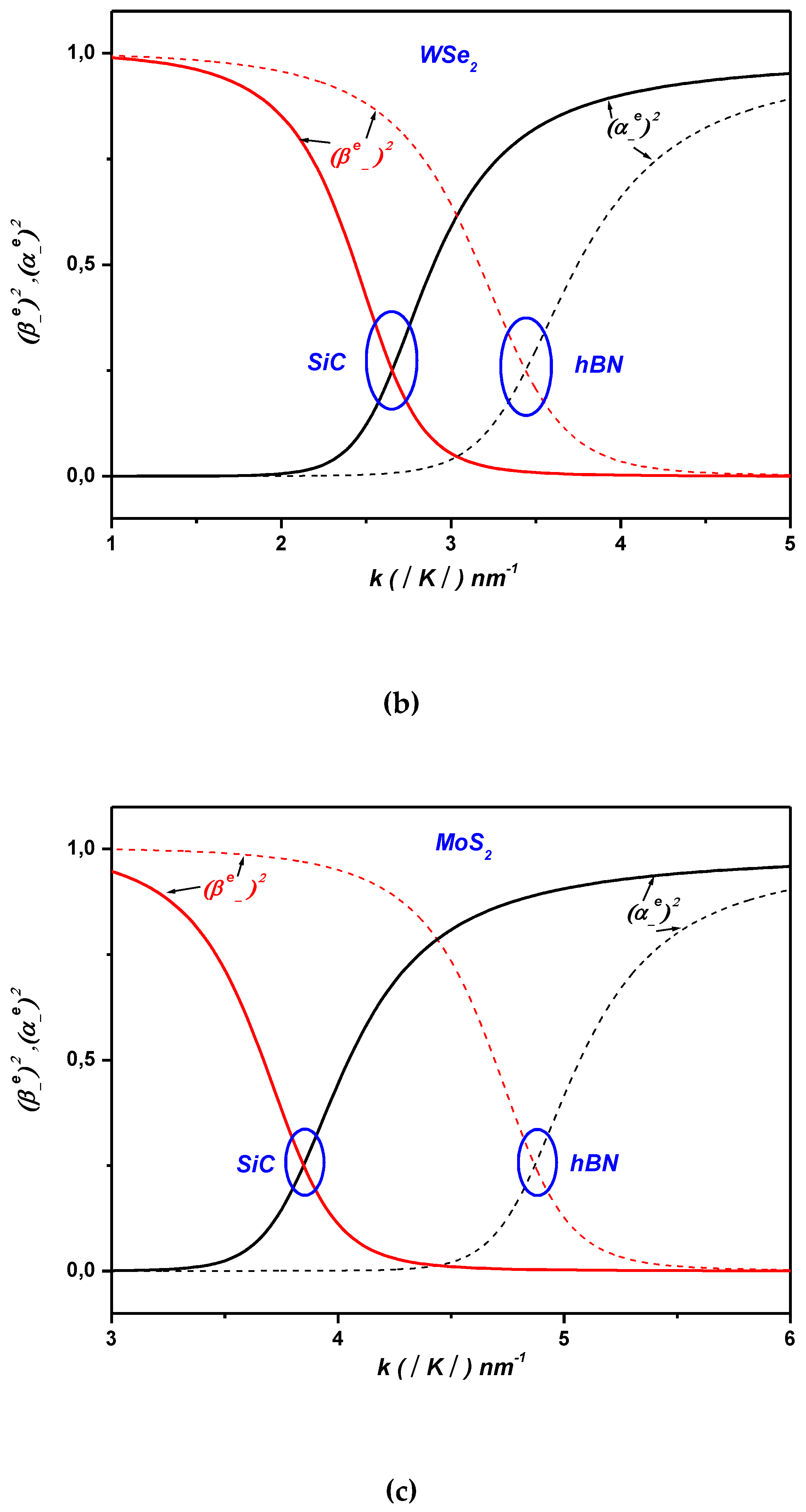
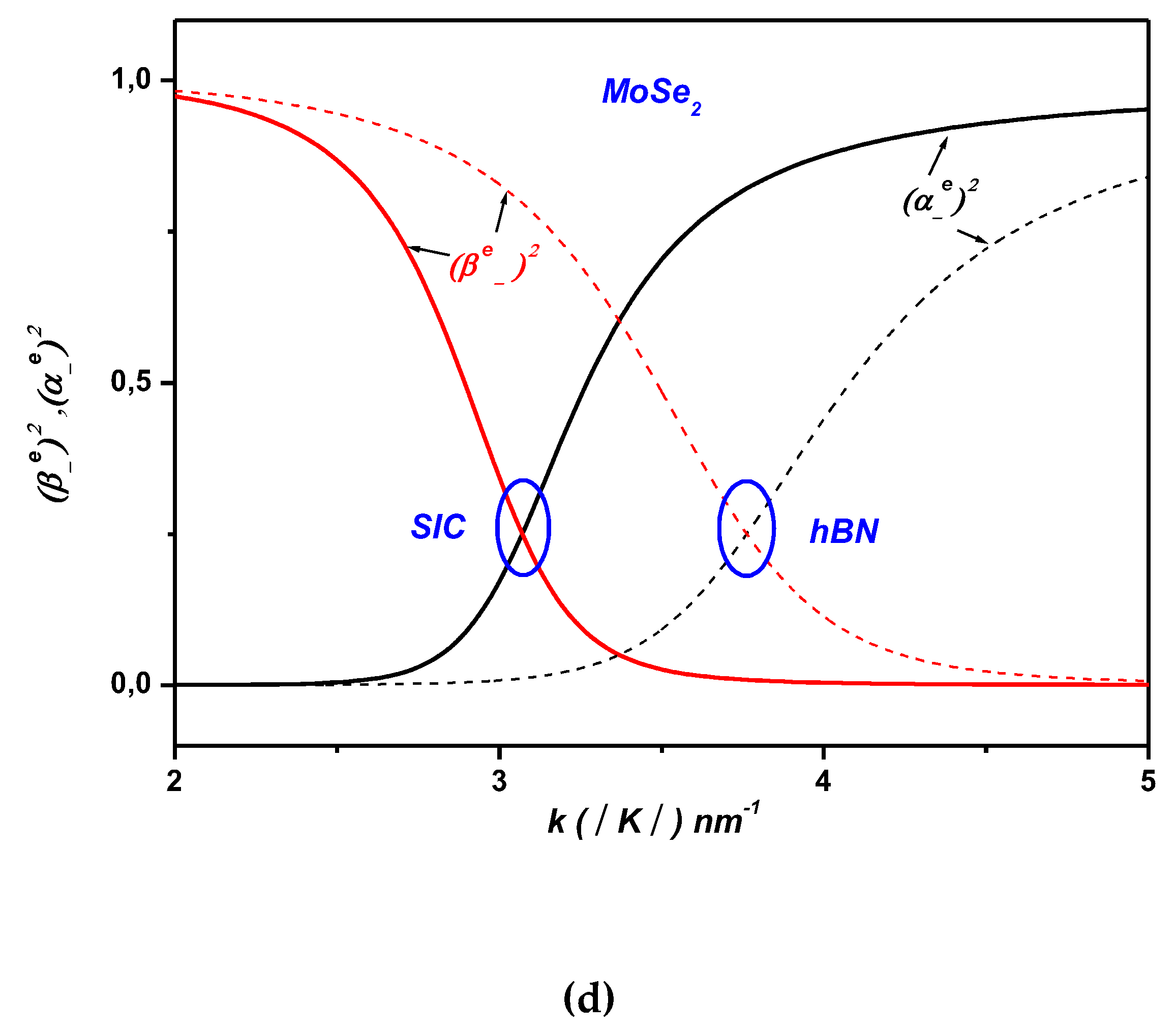
Figure 4, depicts the weight of the electronic components and the one-phonon components of the lower polaron state ψ in ML TMDCs for S i C and h B N polar substrates as a function of the wave vector k   in ML TMDCs. It can be seen for example in the case of W S 2 on S i C polar substrate (see Table 3, Figure 4) that; when the wave vector k approaches k ~ 2.2   n m 1 , the value of the weight of the one-phonon component for the lower polaron state ψ is much larger compared to that of the electronic component β ± α ± . This result demonstrates that the SOP situated at the interface of the ML W S 2 on S i C polar substrate plays a crucial role in the resonant coupling between the noninteracting states ψ k   ,   1 q and ψ k + q   ,   0 q allowing the formation of the polaron states. It can be noted that the same result has been proved for the other cases of ML T M D C s on S i C and h B N polar substrates (see Table 3 and Figure 4).

3. Polaronic Oscillator Strength of ML TMDCs on SiC and hBN Polar Substrates

In the following section, we theoretically investigate the polaronic oscillator strength (OS) which is another crucial quantity. Drawing an analogy to the oscillator strengths of interband transitions in quantum dots, we have computed the OS for interband transitions in ML TMDCs on polar substrates. In the strong confinement limit, the OS is linked to the overlap integral of the polaronic states, ψ 2 by [45,46]:
f O s c = ψ 2 E p 2 E P L  (16)
where E P is the Kane energy and E P L is the emission energy for one-phonon of the ML TMDCs on polar substrates, which is given by:
E P L = ω L O = E g + E e (17)
where E is the lower polaron energy of the exciton, ω L O is the emitted photon energy and E g is the energy gaps of the ML TMDCs.
We have calculated the OS for the lower polaron state ψ which is a linear combination of the two states ψ k + q   ,   0 q   and ψ k   ,   1 q :
ψ = α ψ k + q , 0 q + β ψ k , 1 q (18)
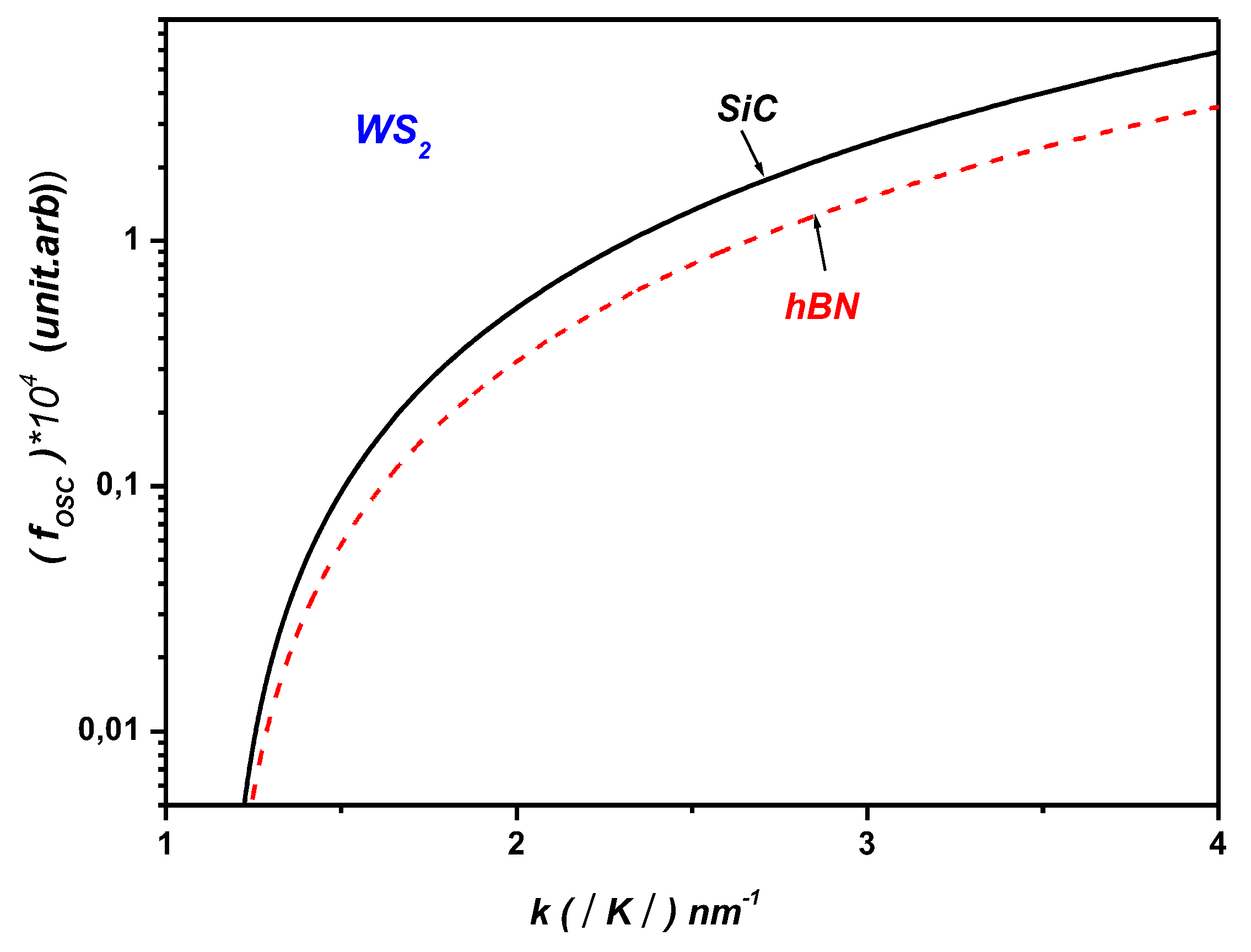
Figure 5 shows the polaronic OS of W S 2 on S i C and h B N polar substrates versus the wave vector k   in ML W S 2 .
As a result, we proved theoretically; that the polaronic OS is especially sensitive to the phonon mode of the surrounding dielectrics. In fact this result is due to the emission energy for one-phonon of the ML TMDCs for S i C and h B N polar substrates, which is given by: E P L =   ω L O = E g + E . Hence, the highest polaronic oscillator strength corresponds to the highest optical phonon energy of the polar substrates E P L =   ω L O . This is by analogy to polaronic oscillator strength in ML TMDCs which is also much higher as compared with conventional semiconductors [6,7,8,9].
Using the same method, we can easily prove that for the other ML TMDCs such as: W S e 2 , M o S 2 , and M o S e 2 :
f O s c M L T D M C s / S i C > f O s c M L T D M C s / h B N . (19)
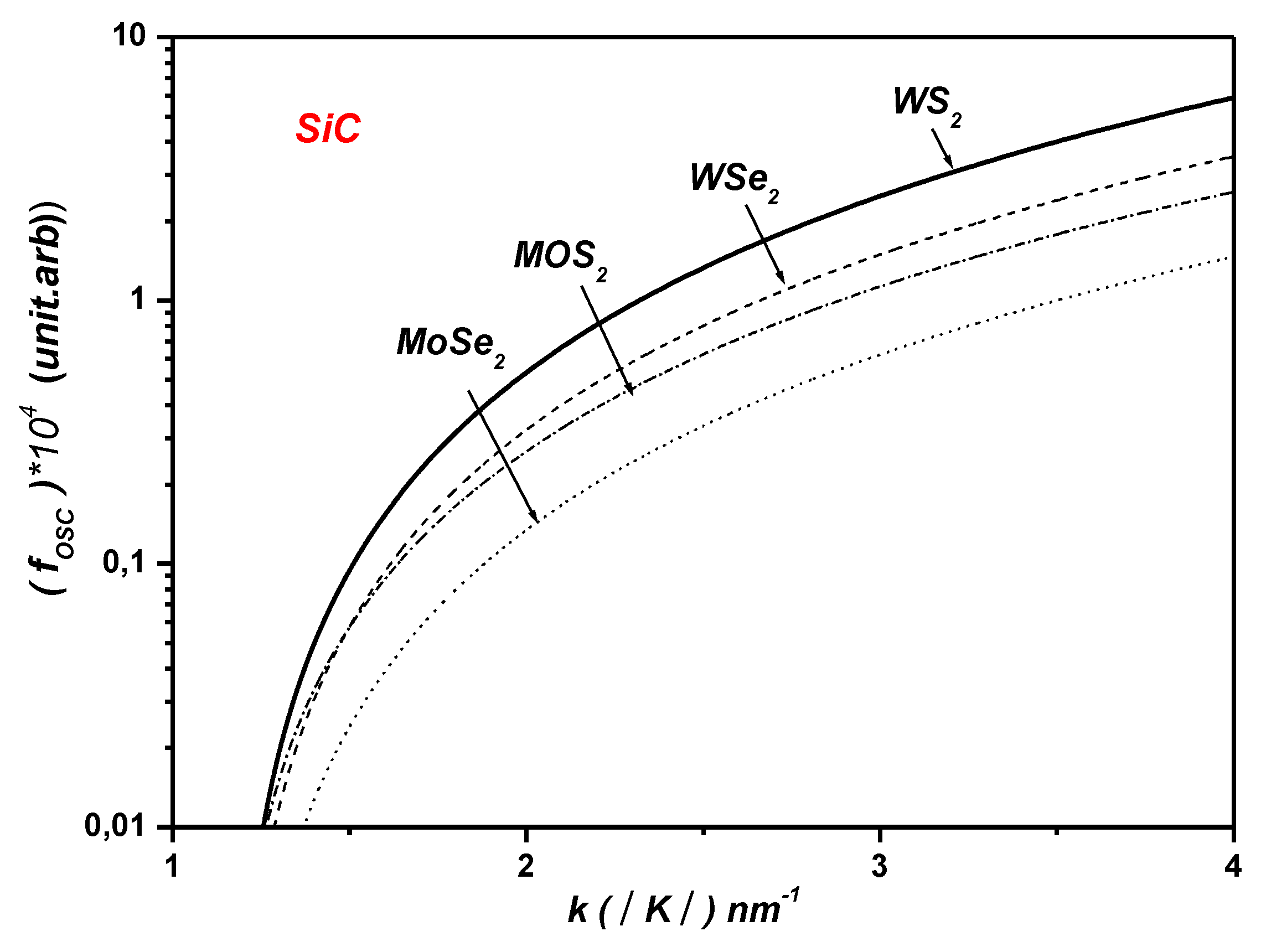
This result is due to the S i C dielectric constant as well as the S i C phonon energy compared to that of h B N   ħ ω L O   S i C = 123.2 m e V > ħ ω L O   h B N = 103.7 m e V , (see Table 1), so the polar field created near the interface should be the highest in the case of S i C substrate, compared to h B N substrate. This result leads to the highest polaronic OS in ML TDMCs on S i C polar substrate. Similarly, it can be concluded from the Figure 6 that:
f O s c W S 2 > f O s c W S e 2 > f O s c M o S 2 > f O s c M o S e 2 . (20)
Hence, this result can be explained by the difference in electron effective masses in ML TDMCs. This result actually confirms the decrement in the polaronic OS for heavy electron in the nearby ML TDMCs / dielectric substrate interface. Otherwise, in the case of light electron, the polaronic OS increases considerably at the strong confinement regime.

4. Polaronic Scattering Rate of ML TMDCs on SiC and hBN Polar Substrates

Now we consider the temperature dependence of the polaronic scattering rate due to the SO phonon. The polaronic scattering rate (SO phonon scattering rate) is given as follow: [17]
1 τ P o l a r o n = 2 π ħ q M k , k + q 2 1 cos θ k θ k + q × × N q δ E k E k + q + ħ ω q + N q + 1 δ E k E k + q ħ ω q  (21)
Here N q is the Bose-Einstein phonon occupation number, θ k   is a directional angle of wave vector k , M k , k + q 2 is given by:
M k , k + q 2 = ψ k V S O P ψ k + q 2 = 1 cos θ k θ k + q 2 4 π 2 e 2 F 2 N 3 2 a 2 q e 2 q z 0  (22)
The summation q is replaced by the integral N A 4 π 2 q d q d θ (sum over a spin and a valley), where   A = 3   2 a 2 is the area of the elementary cell that contains two atoms.
Thus,
1 τ P o l a r o n = 2 π ħ N A 2 π 2 1 cos θ k θ k + q 2 4 π 2 e 2 F ν 2 N A q e 2 q z 0 1 cos θ k θ k + q × × N q δ E k E k + q + ħ ω q + N q + 1 δ E k E k + q ħ ω q q d q d θ q  (23)
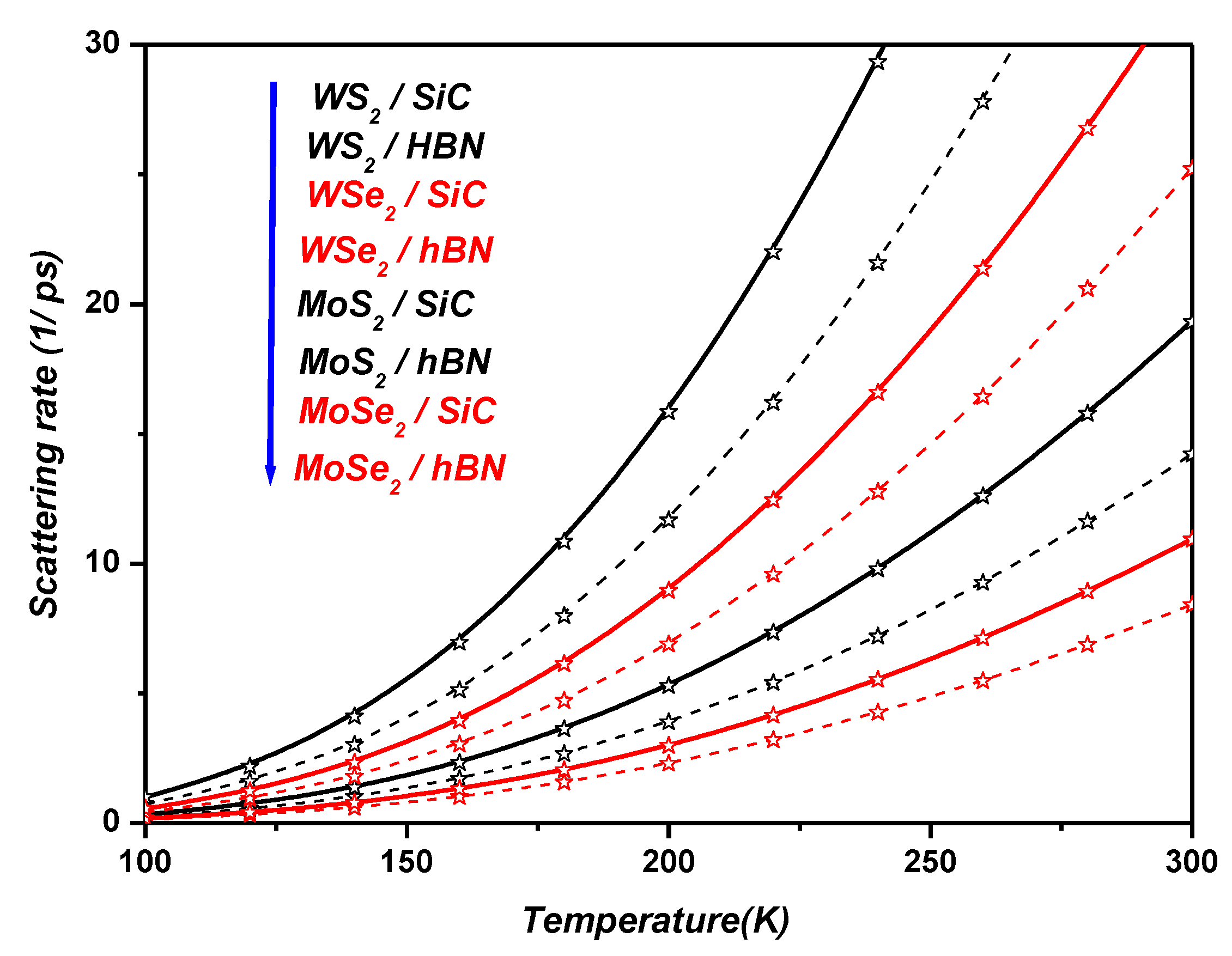
Figure 7 shows the temperature dependence of the SO phonon scattering rate in ML TDMCs on S i C and h B N polar substrates. We clearly see that at temperatures higher than the room temperature, the SO phonon scattering rate increases with temperature, whereas at low temperatures, SO phonon scattering rate is not significant. Similarly, it can be concluded from the Figure 7 that:
1 / τ P o l a r o n W S 2 > 1 / τ P o l a r o n W S e 2 > 1 / τ P o l a r o n M o S 2 > 1 / τ P o l a r o n M o S e 2 . (24)
From Figure 7, we can also observe that the SO phonon scattering rate in ML TDMCs depends strongly on the dielectric constant of the polar substrate, thus:
1 / τ P o l a r o n M L T D M C s / S i C > 1 / τ P o l a r o n M L T D M C s / h B N  (25)
Finally, choosing a suitable dielectric as a substrate one can achieve the highest SO phonon scattering rate in ML TDMCs.
To test experimentally electron-surface optical phonon (SOP) interaction in transition metal dichalcogenides (TMDs) deposited on silicon carbide or hexagonal boron nitride dielectric substrates we propose several experiments such as Photoluminescence (PL) Spectroscopy, Raman Spectroscopy, Time-Resolved Photoluminescence (TRPL), Electroluminescence (EL) Spectroscopy and Angle-Resolved Photoemission Spectroscopy (ARPES) [22,47,48,49,50].

5. Conclusions

In conclusion, our results indicate that the SOP coupling in ML TDMCs depends strongly upon the polar substrate. Moreover, the resonant coupling between electronic sub-levels and surface polar vibration modes, leads to the Rabi splitting of electron levels in single-layer TMDCs. Hence, the polarization field induces a robust, resonant mixing between electronic states and surface vibration modes when their energies become comparable. This resonant coupling has the potential to diminish the probability of nonradiative recombination processes and enhance the efficiency of photoluminescence (PL). Finally, we demonstrate that, the highest polar field created near the interface leads to the highest polaronic OS and the enhancement of SO phonon scattering rates in ML TDMCs. Thus, polaronic OS and polaronic scattering rates depend strongly upon the choice of the polar substrate. The presence of polaronic states may yield significant implications for energy relaxation in ML TMDCs. Moreover, the interaction between electrons and surface optical phonons is a crucial factor influencing the physical characteristics of 2D semiconductors, particularly influencing processes like phonon-assisted hot carrier relaxation.

Author Contributions

Conceptualization, visualization M.M., R.B.., and S.G.; methodology, M.M; investigation, formal analysis, M.M..; writing—original draft preparation, M.M.; writing—review and editing, M.M.., R.B.., and S.G..; supervision, S.G. All authors have read and agreed to the published version of the manuscript.

Institutional Review Board Statement

Not applicable.

Informed Consent Statement

Not applicable.

Data Availability Statement

The data presented in this study are available on request from the corresponding author. The data are not publicly available due to privacy issues.

Conflicts of Interest

The authors declare no conflict of interest.

References

  1. Zixuan Wang ; Yecheng Nie ; Haohui Ou ; Dao Chen ; Yingqian Cen ; Jidong Liu ; Di Wu ; Guo Hong ; Benxuan Li ; Guichuan Xing ; and Wenjing Zhang. Electronic and Optoelectronic Monolayer WSe2 Devices via Transfer-Free Fabrication Method. Nanomaterials 2023, 13, 1368. [CrossRef]
  2. Tanveer Ahmed ; Jiajia Zha; Kris KH Lin; Hao-Chung Kuo ; Chaoliang Tan, Der-Hsien . Bright and Efficient Light-Emitting Devices Based on 2D Transition Metal Dichalcogenides. Advanced Materials 2023, 35, 2208054. [CrossRef]
  3. Saju Joseph ; Jainy Mohan ; Seetha Lakshmy ; Simil Thomas ; Brahmananda Chakraborty ; Sabu Thomas ; Nandakumar Kalarikkal. A review of the synthesis, properties, and applications of 2D transition metal dichalcogenides and their heterostructures. Materials Chemistry and Physics 2023, 297, 127332. [CrossRef]
  4. Chit Siong Lau; Jing Yee Chee; Liemao Cao ; Zi-En Ooi ; Shi Wun Tong ; Michel Bosman ; Fabio Bussolotti ; Tianqi Deng ; Gang Wu, Shuo-Wang Yang, and al.. Gate-Defined Quantum Confinement in CVD 2D WS2. Advanced Materials 2022 , 34, 2103907. [CrossRef]
  5. Lifu Zhang; Ruihao Ni; You Zhou . Controlling quantum phases of electrons and excitons in moiré superlattices. J. Appl. Phys 2023, 133, 080901. [CrossRef]
  6. Vincenzo Ardizzone; Luisa De Marco; Milena De Giorgi; Lorenzo Dominici; Dario Ballarini and Daniele Sanvitto. Emerging 2D materials for room-temperature polaritonics. Nanophotonics 2019, 8, 1547–1558. [CrossRef]
  7. Kaichen Xie ; Xiaosong Li, and Ting Cao. Theory and Ab Initio Calculation of Optically Excited States—Recent Advances in 2D Materials. Advanced Materials 2021, 33, 1904306. [CrossRef]
  8. Maurizia Palummo ; Marco Bernardi ; Jeffrey C Grossman. Exciton Radiative Lifetimes in Two-Dimensional Transition Metal Dichalcogenides. Nano Letters 2015, 15, 2794–2800. [CrossRef]
  9. Diana Y. Qiu; Ting Cao; and Steven G. Louie, Nonanalyticity, Valley Quantum Phases, and Lightlike Exciton Dispersion in Monolayer Transition Metal Dichalcogenides: Theory and First-Principles Calculations. Phys. Rev. Lett 2015. 115, 176801. [CrossRef]
  10. Chung-Che Huang; He Wang; Yameng Cao; Ed Weatherby; Filipe Richheimer; Sebastian Wood; Shan Jiang; Daqing Wei; Yongkang Dong; Xiaosong Lu; and al.. Facilitating Uniform Large-Scale MoS2, WS2 Monolayers, and Their Heterostructures through van der Waals Epitaxy. ACS Appl.Mater.Interfaces 2022, 14, 42365−42373. [CrossRef]
  11. Naoki Wada; Jiang Pu; Yuhei Takaguchi; Wenjin Zhang; Zheng Liu; Takahiko Endo; Toshifumi Irisawa; Kazunari Matsuda; Yuhei Miyauchi; Taishi Takenobu; Yasumitsu Miyata. Efficient and Chiral Electroluminescence from In-Plane Heterostructure of Transition Metal Dichalcogenide Monolayers. Advanced Functional Materials 2022 ,32, 2203602. [CrossRef]
  12. C. Robert; B. Han ; P. Kapuscinski ; A. Delhomme ; C. Faugeras ; T. Amand ; M. R. Molas ; M. Bartos ; K. Watanabe ; T. Taniguchi ; B. Urbaszek ; M. Potemski ; and X. Marie. Measurement of the spin-forbidden dark excitons in MoS2 and MoSe2 monolayers. Nature Communications. 2020, 11, 4037. [CrossRef]
  13. Carrascoso, F. ; Li, H., Frisenda ; R. et al. . Strain engineering in single-, bi- and tri-layer MoS2, MoSe2, WS2 and WSe2. Nano Research 2021 , 14, 1698–1703. [CrossRef]
  14. M. Mahdouani. Investigation of the electron-surface phonon interaction effects in graphene on a substrate made of polar materials . PHYSE 2017, 87, 192-198. [CrossRef]
  15. M. Mahdouani; S. Gardelis; R. Bourguiga. The effect of Si impurities on the transport properties and the electron-surface phonon interaction in single layer graphene deposited on polar substrates. Physica B: Condensed Matter. 2018, 550, 171–178. [CrossRef]
  16. M.Mahdouani; R. Bourguiga. Auger and carrier-surface phonon interaction processes in graphene on a substrate made of polar materials. Superlattices and Microstructures. 2017, 102, 212–220. [CrossRef]
  17. Vasili Perebeinos; Phaedon Avouris. Inelastic scattering and current saturation in graphene. PHYSICAL REVIEW B 2010, 81, 195442. [CrossRef]
  18. M. Mahdouani; R. Bourguiga; and S. Jaziri. Polaronic states in Si nanocrystals embedded in SiO2 matrix. Physica E 2008, 41, 228-234. [CrossRef]
  19. M.Mahdouani; S.Gardelis; and A.G.Nassiopoulou. Role of surface vibration modes in Si nanocrystals within light emitting porous Si at the strong confinement regime. J. Appl. Phys 2011, 110, 023527. [CrossRef]
  20. S. Gardelis ; A.G. Nassiopoulou; M. Mahdouani; R. Bourguiga; S. Jaziri. Enhancement and red shift of photoluminescence (PL) of fresh porous Si under prolonged laser irradiation or ageing: Role of surface vibration modes. Physica E. 2009, 41, 986–989. [CrossRef]
  21. Suvodeep Paul ; Saheb Karak ; Saswata Talukdar ; Devesh Negi and Surajit Saha. Influence of Edges and Interlayer Electron–phonon Coupling in WS2/h-BN Heterostructure. ACS Appl. Mater. Interfaces 2024, 16, 40077–40085. [CrossRef]
  22. Colin, M. Chow; Hongyi Yu; Aaron M. Jones; Jiaqiang Yan; David G. Mandrus; Takashi Taniguchi; Kenji Watanabe; Wang Yao; Xiaodong Xu. Unusual Exciton–Phonon Interactions at van der Waals Engineered Interfaces. Nano Lett 2017, 17, 1194–1199. [Google Scholar] [CrossRef]
  23. Bastian Miller; Jessica Lindlau; Max Bommert; Andre Neumann; Hisato Yamaguchi,Alexander Holleitner; Alexander Högele & Ursula Wurstbauer. Tuning the Fröhlich exciton-phonon scattering in monolayer MoS2. Nature Communications 2019, 10, 807. [CrossRef]
  24. Sanjay Gopalan; Maarten L. Van de Put; Gautam Gaddemane; and Massimo V. Fischetti. Theoretical Study of Electronic Transport in Two-Dimensional Transition Metal Dichalcogenides: Effects of the Dielectric Environment. Phys. Rev. Applied. 2022, 18, 054062. [CrossRef]
  25. M. M. Glazov; and E. L. Ivchenko. Valley Orientation of Electrons and Excitons in Atomically Thin Transition Metal Dichalcogenide Monolayers. JETP Letters. 2021, 113, 7–17. [CrossRef]
  26. M. V. Durnev and M. M. Glazov. Excitons and trions in two-dimensional semiconductors based on transition metal dichalcogenides. Physics–Uspekhi. 2018, 61, 825–845. [CrossRef]
  27. Kormanyos; G. Burkard; M. Gmitra, J. Fabian; V. Zolyomi; N. D. Drummond; and V. Fal’ko. k·p theory for two-dimensional transition metal dichalcogenide semiconductors. 2D Mater. 2015, 2, 022001. [CrossRef]
  28. Gabriel Antonius and Steven, G. Louie. Theory of exciton-phonon coupling. Phys. Review B 2022, 105, 085111. [Google Scholar] [CrossRef]
  29. Thibault Sohier; Matteo Calandra; and Francesco Mauri. Two-dimensional Fröhlich interaction in transition-metal dichalcogenide monolayers: Theoretical modeling and first-principles calculations. Phys. Rev. B 2016, 94, 085415. [CrossRef]
  30. Yixiong Wang ; Chenglin He ; Qin Tan ; Zilan Tang ; Lanyu Huang ; Liang Liu ; Jiaocheng Yin,Ying Jiang ; Xiaoxia Wang and Anlian Pan. Exciton–phonon coupling in two-dimensional layered (BA)2PbI4 perovskite microplates, RSC Adv. 2023, 13, 5893–5899. [CrossRef]
  31. Jinlong Ma; Dongwei Xu; Run Hu ; Xiaobing Luodoi. Examining two-dimensional Fröhlich model and enhancing the electron mobility of monolayer InSe by dielectric engineering. Journal of Applied Physics 2020, 128, 035107. [CrossRef]
  32. Nicki Frank Hinsche and Kristian Sommer Thygesen. Electron–phonon interaction and transport properties of metallic bulk and monolayer transition metal dichalcogenide TaS2. 2D Materials 2017, 5, 015009. [CrossRef]
  33. Xiao; Y., Li, Z.Q.; Wang, Z.W. Polaron effect on the bandgap modulation in monolayer transition metal dichalcogenides. J. Phys. Cond. Matter 2017, 29 , 485001. [CrossRef]
  34. J. V. Nguepnang ; C. Kenfack-Sadem ; A. Kenfack-Jiotsa ; M. F. C. Fobasso ·Y. Sun. Optical signature of bipolaron in monolayer transition metal dichalcogenides: all coupling approach. Optical and Quantum Electronics. 2021, 53, 728. [CrossRef]
  35. Devreese, J.T.; Huybrechts, W.; Lemmeks, L. On the optical absorption of free polarons at weak coupling. Physica Status Solidi (b) 1971, 48, 77–86. [CrossRef]
  36. Daniela, L. Mafra and Paulo T. Araujo. Intra- and Interlayer Electron-Phonon Interactions in 12/12C and 12/13C BiLayer Graphene. Appl. Sci. 2014, 4, 207–239 . [Google Scholar] [CrossRef]
  37. S. Q. Wang and G. D. Mahan. Electron Scattering from Surface Excitations .Phys. Rev. B. 1972, 6, 4517. [CrossRef]
  38. A. V. Rozhkov ; Franco Nori. Exact wave functions for an electron on a graphene triangular quantum dot. PHYSICAL REVIEW B. 2010, 81, 155401. [CrossRef]
  39. J¨urgen Schiefele, Fernando Sols, and Francisco Guinea, Temperature dependence of the conductivity of graphene on boron nitride. Phys. Rev. B 2012, 85, 195420. [CrossRef]
  40. R. Geick; C. H. Perry; and G. Rupprecht. Normal Modes in Hexagonal Boron Nitride. Phys. Rev. 1966, 146, 543. [CrossRef]
  41. B. Han; C. Robert; E. Courtade; M. Manca; S. Shree; T. Amand; P. Renucci; T. Taniguchi; K. Watanabe; X. Marie; L. E. Golub; M. M. Glazov; and B. Urbaszek1. Exciton States in Monolayer MoSe2 and MoTe2 Probed by Up conversion Spectroscopy. PHYSICAL REVIEW X. 2018, 8, 031073. [CrossRef]
  42. G. Wang; I. C. Gerber; L. Bouet ; D. Lagarde; A. Balocchi; M. Vidal; E. Palleau; T. Amand; X. Marie; and B. Urbaszek. Exciton states in monolayer MoSe2: impact on interband transitions . 2D Materials. 2015, 2, 045005. [CrossRef]
  43. Akash Laturia; Maarten L. Van de Put. and William G. Vandenberghe. Dielectric properties of hexagonal boron nitride and transition metal dichalcogenides: from monolayer to bulk. 2D Materials and Applications. 2018, 2, 6. [CrossRef]
  44. L.X.Benedict; S. G. Louie; and M. L. Cohen. Static polarizabilities of single-wall carbon nanotubes. Phys. Rev. B. 1995, 52, 8541. [CrossRef]
  45. E. H. Hwang and S. Das Sarma . Surface polar optical phonon interaction induced many-body effects and hot-electron relaxation in graphene. Phys.Rev.B. 2013, 87, 115432. [CrossRef]
  46. Mounira Mahdouani; Meriam Zalfani; Ramzi Bourguiga; Bao-Lian Su. Radiative and non radiative recombinations study in the novel nanocomposites BiVO4/3DOM-TiO2, ZnO/3DOM-TiO2 and BiVO4/3DOM-ZnO: Application to the photocatalysis. Physica E: Low-dimensional Systems and Nanostructures 2019, 108, 269–280. [CrossRef]
  47. Yu-Chen Chang; Yu-Chiao Chan; Bipul Das; Jiao-Fang Syue; Hsiang-Chi Hu, Yann-Wen Lan; and Ting-Hua L. Distinctive characteristics of exciton-phonon interactions in optically driven MoS2. Phys. Rev. Materials 2024, 8, 074003. [CrossRef]
  48. J. V. Nguepnang ; C. Kenfack-Sadem ; A. Kenfack-Jiotsa; C. Guimapi; A. J. Fotue &; A. E. Merad. Electron–phonon coupling contribution on the optical absorption and the dynamic of exciton-polaron in monolayer Transition Metal Dichalcogenides. Optical and Quantum Electronics. 2021, 53, 654. [CrossRef]
  49. Jia-Min Lai, Ya-Ru Xie, Jun Zhang, Detection of electron-phonon coupling in two-dimensional materials by light scattering. Nano Res. 2021, 14, 1711–1733. [CrossRef]
  50. Ying Jiang ; Shula Chen; Weihao Zheng; Biyuan Zheng and Anlian Pan. Interlayer exciton formation, relaxation, and transport in TMD van der Waals heterostructures. Light: Science & Applications 2021, 10, 72. [CrossRef]
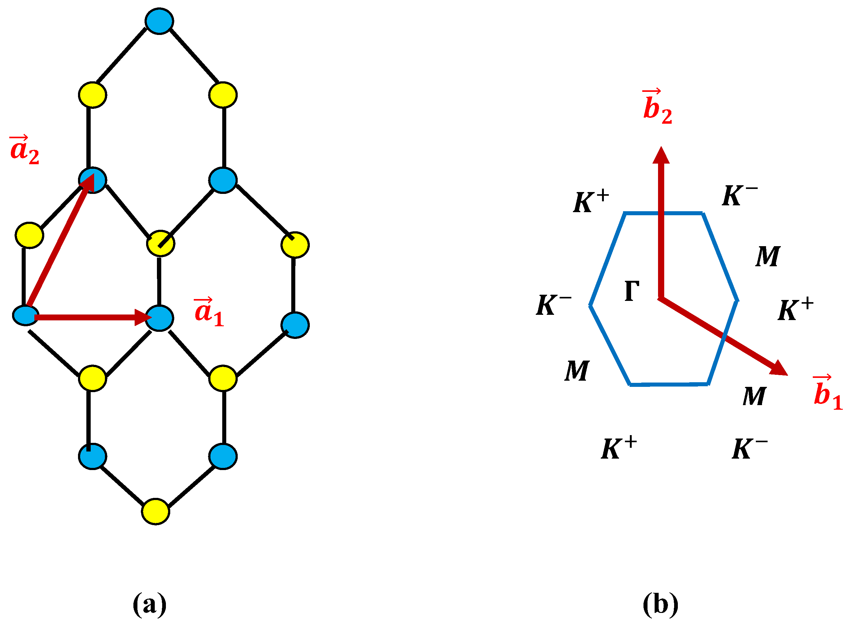
Figure 1. (a) The triangular Bravais lattice of monolayer transition-metal dichalcogenides MX2. Blue and yellow spheres denote the metal (M) and chalcogenide (X) atoms, respectively. (b) The first Brillouin zone and high-symmetry points Γ , K , and M of TMDCs in reciprocal space of the triangular lattice. Its primitive lattice vectors are b 1 and b 2 .
Preprints 120879 g001
Figure 2. The SO coupling strength between the electronic states ψ k   and ψ k + q   versus the wave vector k   in ML WS2 on S i C and h B N polar substrates.
Preprints 120879 g002
Figure 3. Polaron electron energies as a function of the wave vector k :   (a) in ML W S 2   ,   W S e 2   ,   M o S 2   a n d   M o S e 2 on S i C polar substrate; (b) in ML W S 2   ,   W S e 2   ,   M o S 2   a n d   M o S e 2 on h B N polar substrate.
Preprints 120879 g003aPreprints 120879 g003bPreprints 120879 g003cPreprints 120879 g003d
Figure 4. The weight of the electronic components and the one-phonon components of the lower polaron state ψ in ML TMDCs on S i C and h B N dielectric substrates, (a) in W S 2 , (b) in W S e 2 , (c) in M o S 2   and (d) in M o S e 2 versus the wave vector k .
Preprints 120879 g004aPreprints 120879 g004bPreprints 120879 g004c
Figure 5. Polaronic OS of W S 2 on S i C and h B N polar substrates versus the wave vector k   in ML W S 2 .
Preprints 120879 g005
Figure 6. Polaronic OS in ML W S 2   ,   W S e 2   ,   M o S 2   a n d   M o S e 2 on S i C and h B N polar substrates versus the wave vector k   in ML W S 2 .
Preprints 120879 g006
Figure 7. Temperature dependence of the SO phonon scattering rate in ML W S 2   ,   W S e 2   ,   M o S 2   a n d   M o S e 2 on S i C and h B N polar substrates.
Preprints 120879 g007
Table 1. Parameters for the surface polar phonons scattering of ML TMDCs on S i C and h B N polar substrate.
Preprints 120879 i001
Table 2. The band gap, effective electron mass and the internal distance between the TMDCs and polar substrate.
Preprints 120879 i002
Table 3. The crossing values k of the noninteracting states ψ k , 1 q a n d ψ k + q , 0 q in the ML W S 2 , W S e 2 , M o S 2 a n d M o S e 2 for both S i C and h B N polar substrates.
Preprints 120879 i003
Table 4. The Rabi splitting of the electron levels in the ML W S 2   ,   W S e 2   ,   M o S 2   a n d   M o S e 2 for both S i C and h B N polar substrates.
Preprints 120879 i004
Disclaimer/Publisher’s Note: The statements, opinions and data contained in all publications are solely those of the individual author(s) and contributor(s) and not of MDPI and/or the editor(s). MDPI and/or the editor(s) disclaim responsibility for any injury to people or property resulting from any ideas, methods, instructions or products referred to in the content.
Copyright: This open access article is published under a Creative Commons CC BY 4.0 license, which permit the free download, distribution, and reuse, provided that the author and preprint are cited in any reuse.
Prerpints.org logo

Preprints.org is a free preprint server supported by MDPI in Basel, Switzerland.

Subscribe

© 2024 MDPI (Basel, Switzerland) unless otherwise stated