1. Introduction
Gas meters are indispensable measurement devices in modern urban infrastructure, widely used for quantifying gas consumption in residential and industrial environments [
1,
2]. With the rapid advancement of smart cities (where every single natural person in the city is managed by the government in order to provide intelligent service to all residents as a whole [
3]), the role and significance of gas meters in energy management and intelligent monitoring have become increasingly prominent. The quality of gas meters directly affects the accuracy of gas measurement and the safety of users [
4,
5,
6]. The control printed circuit board (PCB) of a gas meter, serving as its core component, is responsible for critical functions such as data processing, signal transmission, and control execution. The manufacturing quality of this PCB decisively influences the reliable operation of the gas meter. Therefore, ensuring the manufacturing quality of the gas meter’s control PCB is central and crucial to quality assurance in gas meter manufacturing [
7,
8].
The quality issues of gas meter control PCBs primarily arise from various defects during the manufacturing process, such as poor welding, component misplacement, and circuit breaks [
9,
10,
11]. Among these, the detection precision of dynamic defects during manufacturing is the key factor determining the final product quality. Consequently, research focusing on enhancing the detection precision of dynamic defects in PCBs has become a hot spot in the field of defect detection.
Current research methodologies for PCB defect detection mainly include machine vision-based methods and deep learning algorithms [
12,
13,
14]. Machine vision-based methods typically employ image processing techniques to identify surface defects on PCBs by comparing captured images with reference images. While these methods are straightforward and computationally efficient, they often lack the precision required to detect subtle defects, especially in complex or noisy backgrounds [
15]. Moreover, they generally do not provide information that can guide the tracing of defects back to specific stages in the manufacturing process or inform effective repair strategies.
Deep learning approaches, such as those based on convolutional neural networks (CNNs), have been proposed to improve detection precision by learning complex patterns from large datasets [
16,
17]. These methods can achieve high accuracy in defect detection and classification. However, they require extensive training on large, labeled datasets, which can be time-consuming and costly to obtain. Additionally, deep learning models often act as black boxes, providing limited interpretability, which hinders their ability to guide defect tracing or repair in the manufacturing process.
In summary, existing research inadequately addresses the challenges of achieving high detection precision without the need for large training datasets and providing actionable insights for defect tracing and repair. Most methods focus solely on defect detection without offering the ability to analyze the discrepancies between the detected image and the desired image in a way that can inform corrective actions in the manufacturing process. This limitation hampers the ability to improve manufacturing processes based on the detection results.
To address these challenges, this paper proposes a melding defect detection method for PCBs in gas meters based on discrete optimal transport (as introduced in
Section 2.3, the solution to a convex linear program introduced by Kantarovich [
18]). The proposed method is an image comparison approach that contrasts the gathered images of the detecting areas with standard or desired images. Since solving discrete optimal transport problems can become computationally expensive, particularly when dealing with high-resolution images, our method mitigates this issue by focusing solely on the welding areas of the PCB. This localized analysis significantly reduces computational cost while maintaining precision. By utilizing discrete optimal transport theory, the method calculates the optimal mass flow between the detected image and the reference image, enabling precise identification of discrepancies in the welding areas. This high detection precision does not rely on large datasets for training, making it more practical for industrial applications where labeled data may be scarce. Furthermore, the calculated mass flow provides valuable information about the nature and extent of the defects, which can be used as a guide to trace back to potential issues in the manufacturing process and to inform subsequent repairs. This approach overcomes the limitations of existing methods by combining superior detection precision, minimal data requirements, relative low computational cost, and actionable insights for manufacturing process improvement and product repair, thereby offering a robust solution for quality assurance in gas meter manufacturing.
The specific structure of this paper is as follows: The literature review and related work are shown in
Section 2. The problem definition and mathematical formulation are established in
Section 3. The solver design to solve the optimal transport problem is presented in
Section 4. The introduction for the welding defect detection method based on discrete optimal transport is described in
Section 5. The experimental results and analysis are provided in
Section 6. The conclusion to this paper is given in
Section 7.
2. Literature Review and Related Work
2.1. Machine Vision-Based Methods
Machine vision has been widely used for PCB defect detection due to its ability to offer real-time monitoring and non-contact inspection at relatively low cost. Baygin et al. proposed a machine vision-based algorithm for detecting missing components and solder joint issues, demonstrating reliable detection in well-lit environments [
14]. Similarly, Chang et al. applied machine vision techniques to detect soldering defects in PCBs, contributing to the faster and more cost-effective detection of welding problems [
15].
Despite these benefits, machine vision approaches often struggle with precision, particularly when handling smaller or subtle defects. Liu and Qu found that in noisy environments, machine vision systems often fail to detect minor welding defects, leading to inaccuracies [
19]. Ren et al. also noted that traditional machine vision systems face limitations in real-world conditions, such as variable lighting and background noise, which can compromise their detection accuracy [
20]. Additionally, Baygin et al. highlighted that these systems provide little insight into the root causes of defects, making it difficult for manufacturers to trace issues back to their source [
14].
Furthermore, Liao et al. emphasized that traditional machine vision methods often require manual tuning for different PCB designs, limiting their scalability in modern high-throughput production environments [
21]. Despite their speed and cost advantages, these limitations make machine vision less suitable for environments requiring high precision in detecting subtle welding defects.
2.2. Deep Learning-Based Methods
Deep learning approaches, particularly convolutional neural networks (CNNs), have now become increasingly popular for PCB welding defect detection due to their ability to recognize complex patterns and achieve higher precision. Chen et al. demonstrated the effectiveness of deep learning-based models in detecting subtle defects in PCBs, achieving more than 95% accuracy [
12]. Similarly, Legon et al. used CNN-based models to classify PCB defects, improving both detection accuracy and speed [
22]. Liu et al. proposed a deep learning model that leveraged generative adversarial networks (GANs) to improve the resolution of PCB defect images, further enhancing detection performance [
23].
However, deep learning models come with significant drawbacks. Ling et al. pointed out that these models are highly data-dependent, requiring large labeled datasets to perform effectively, which is a challenge in industrial environments where labeled defect data is scarce [
24]. Pham et al. also emphasized the difficulties of acquiring enough training data, noting that deep learning models struggle when the dataset is small or unbalanced [
25].
Moreover, the black-box nature of deep learning algorithms poses interpretability issues, as described by Sezer and Altan. This makes it difficult for manufacturers to understand the root causes of detected defects and to implement targeted repairs [
10]. Although deep learning models significantly improve detection precision, their dependence on large datasets and lack of transparency make them challenging to deploy in many real-world manufacturing environments.
2.3. Optimal Transport
2.3.1. Monge’s Problem
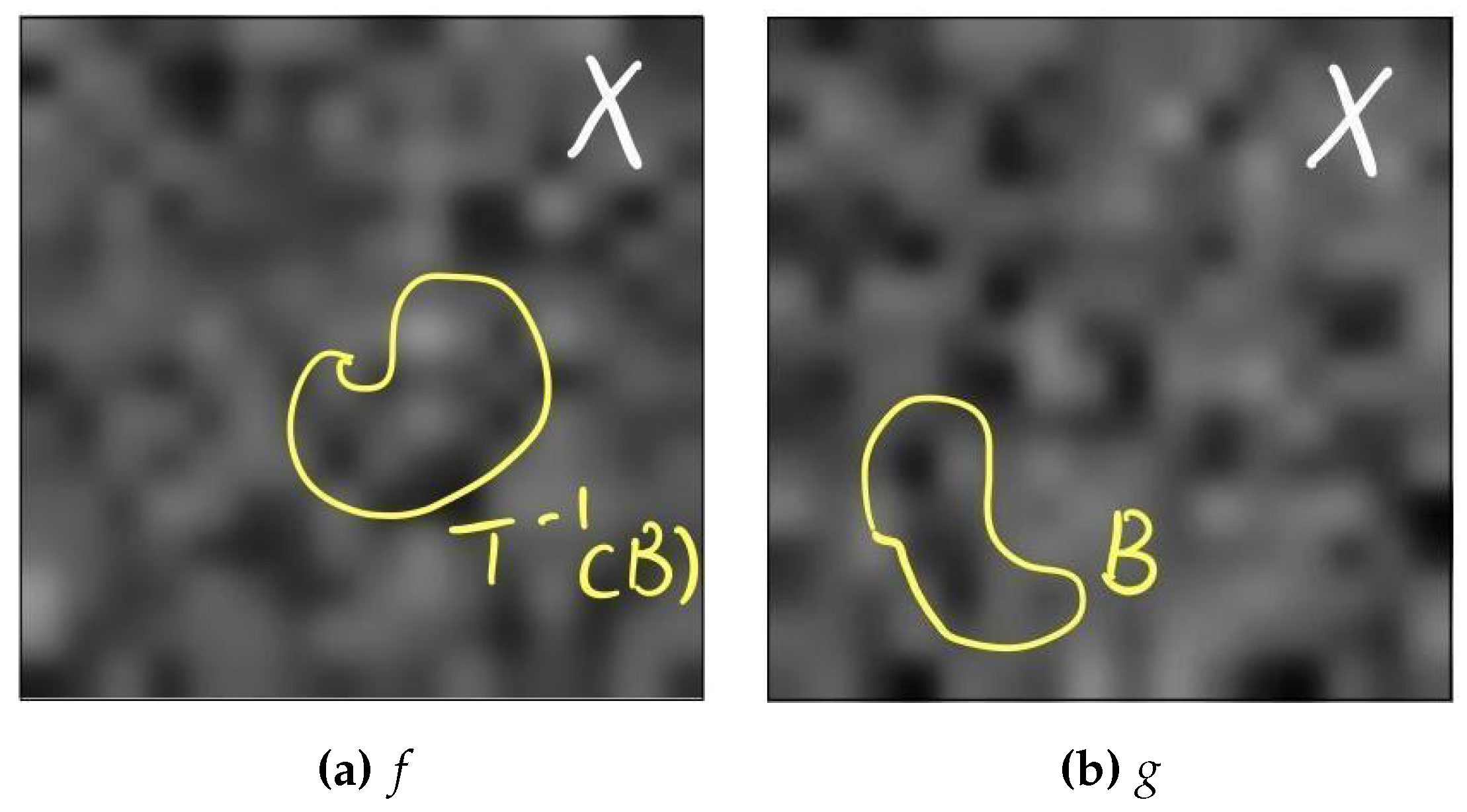
The concept of optimal transport can be traced back to the period right before the French revolution. At that time, Monge proposed an intuitive idea of the optimal transport problem in a very practical reason: how to move a terrain from a given current landscape into another desired landscape with the least amount of total work done [
26].
The initial formulation of the problem is as follows:
where
and
represents the current and desired landscape (as shown in
Figure 1). Since the terrain does not change in size,
must satisfy
.
represent the work of transporting
a to
b is convex.
However, since the function
are zero everywhere except in the landscape, the integral over
X will lead to zero, thus the mass conservation constraint cannot be properly expressed. To solve this problem, replacing with measure instead is helpful. By using sum of weighted dirac masses to represent terrain, the problem can be solved. Then the Monge’s problem with measure is formulated as follows:
where
are measurable, and
are two measures on
respectively, and the cost function
c is convex. Note that the constraint
is the same as saying
g is the push forward of
f by
T,
2.3.2. Kantorovitch’s Relaxed Problem
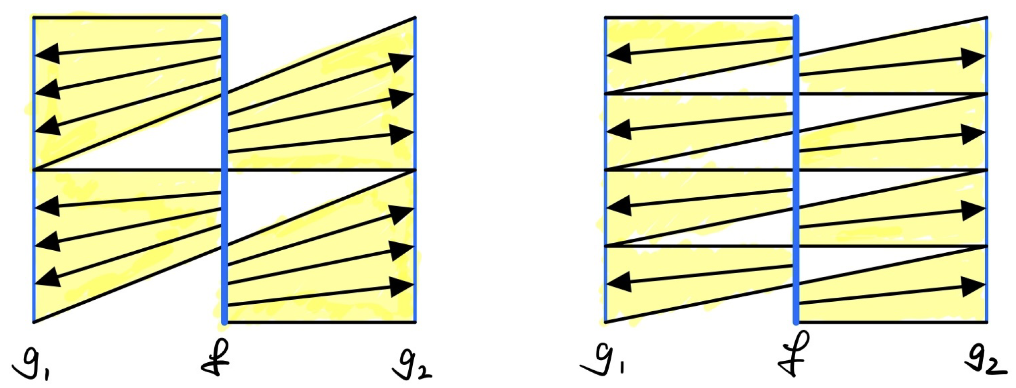
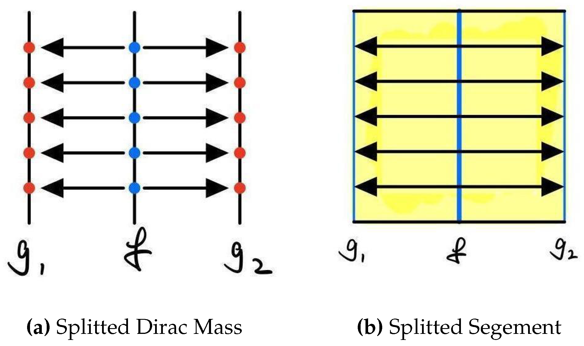
Nevertheless, the Monge’s problem with measure has a problem that the mass cannot be splited or merged as shown in
Figure 2. To solve it, Kantarovich introduced the idea of marginal and relaxed the problem into the following form [
27]:
where
Here
, a measure on the product of space
with marginal
, represents a transport plan between two measures
on
. And
is the projection map, so as
. Note that the space of transport plans
is convex.
In this case, in contrast with
Figure 2, the Kantorovitch’s relaxed problem allows mass to be splitted, and we can have optimal transport transport as shown in
Figure 3.
2.3.3. Discrete Optimal Transport in 1D with Finite Element
The discrete optimal transport problem in 1D with finite element can be easily driven from the Kantarovich’s relaxed problem as follows:
where (i)
are the vectors representing measures on
. (ii)
represents the transport plan which transport
amount of mass from
to
. (iii)
represents the unit cost of transporting from
to
. (iv)
represents the constraints to satisfy marginal. (v)
is some function that flatten matrix
into vector
. Note that flatten function is one-to-one.
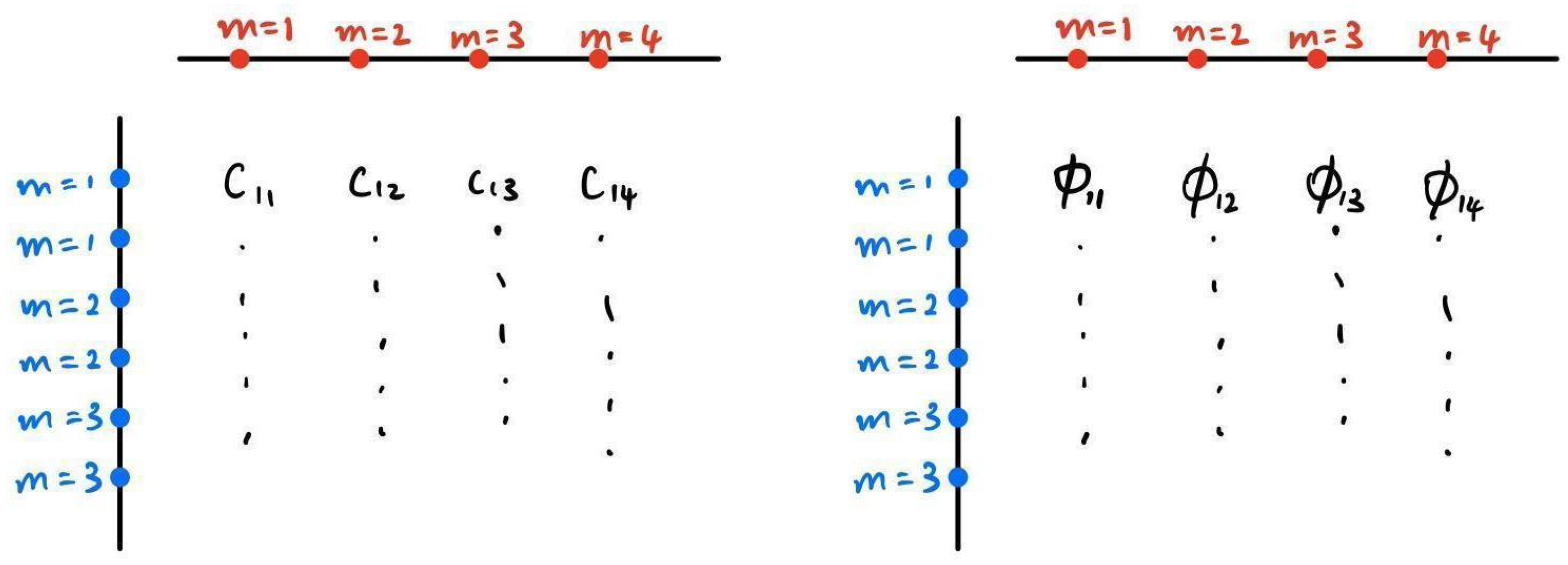
For example, as shown in
Figure 4, the sum of colum of
must equal to the mass above, and the sum of row of
must equal to the mass at the left. The
C is the unit cost of each possible transport pair. The problem is to minimize the cost while satisfying the (1) equality of
and (2) mass above and on the left.
3. Problem Formulation
3.1. Core Problem
The core problem this research seeks to address is the accurate detection of welding defects in PCBs in gas meter while overcoming the limitations of traditional methods. To tackle this problem, we reformulate the PCB welding defect detection challenge as an image comparison task using optimal transport (OT) theory. Specifically:
Input: Two local images—one representing the reference (defect-free) welding area on PCB and the other representing the welding area on PCB under inspection.
Objective: Identify any discrepancies between the reference image and the test image, which may correspond to welding defects.
-
Constraints:
- (a)
Achieving high precision in detecting small, subtle welding defects.
- (b)
Reducing dependency on large, labeled datasets for training detection algorithms
- (c)
Providing interpretability of defect to enable actionable insights for defect tracing, process improvement, and product repair.
3.2. Formulation of Discrete Optimal Transport Problem
We suppose the 2 dimensional image of the detecting image and the reference image are both in the size of
pixels for some
, say
respectively. Since
are in same size, we can easily transform
X to
Y by elementary arithmetic, thus we assume
. Similarly, we assume
Consider the gray scale
for some
represents the brightness of the image, where 0 and
represent the darkest and brightest respectively.
We consider
to be densities on
such that for all
, we have
. By normalizing
, we have the normalized image (density/measure) of the detecting image
f and reference image
g where
Then the optimal transport problem is as follows:
where the cost function
c is the Euclidean distance. If
exist, it is the optimal transport cost and the map
is the optimal transport map.
Table 1.
Notations in Problem Formulation.
Table 1.
Notations in Problem Formulation.
| Notation |
Description |
|
The size in pixel of the input image |
| X |
The 2 dimensional coordinates for each pixel in detecting image |
| Y |
The 2 dimensional coordinates for each pixel in reference image |
|
The set of gray scale |
|
Maximum of gray scale |
|
The measure on X representing the gray sacle detecting image |
|
The measure on Y representing the gray sacle reference image |
| f |
The normalized measure of on X
|
| g |
The normalized measure of on Y
|
|
The optimal cost of transporting f to g
|
3.3. Solvability of the Assignment Problem
Clearly, any
can be considered as
So both
could be considered as some sum of Dirac masses in same scale (
). Note that
which implies that the discrete optimal transport problem could be solved [
18]. This could be cone by algorithm such as transportation simplex [
28], Hungarian [
29], auction [
30], etc.
3.4. Properties of the Assignment Problem
As shown above, the assignment problem has some properties as follows:
To solve the assignment problem does not need any outside information beside the detecting image and reference image.
By solving the assignment, any slight difference between two image would be included in the transport plan and also represented by the optimal transport cost.
The optimal transport plan is two-way since the cost is Euclidean, thus the plan could show that how can the detecting image be transported to the reference image and vice versa.
4. Solver Design
4.1. 2 Dimensional to 1 Dimensional
For further simplicity, we could transform the assignment problem in
Section 3 to 1 dimensional form. We first consider a transform function
such that
Clearly,
is bijective. Denote
, and we let
to be the 1 dimensional frame for images of detecting image and reference image, and we let
to be the 1 dimensional representation of the images where
and
. Then the assignment problem becomes
where
represents the mass transports from
to
Table 2.
Notations in Encoding and Decoding.
Table 2.
Notations in Encoding and Decoding.
| Notation |
Description |
|
The bijective (2D to 1D) flatten function |
| k |
The number of pixels minus one |
|
The 1 dimensional coordinates for the gray scale of both input images |
|
The measure on representing the gray scale detecting image |
|
The measure on representing the gray scale reference image |
|
The unit cost for transporting from ith coordinate to jth coordinate in
|
|
The mass to transport from ith coordinate to jth coordinate in
|
|
The cost of a transport |
|
Mass conservation constraints for detecting image at ith coordinate in
|
|
|
|
Mass conservation constraints for reference image at jth coordinate in
|
|
|
|
The cost map |
|
The transport plan |
|
The constraint matrix which project to vector in
|
|
The constraint vector represents the gray scale at each point for both image |
4.2. Assignment Problem to Linear Programming Problem
Since for any
,
is fixed, we can consider
and
such that
Then we can reformulate the assignment problem as follows
Note that the problem here is a standard linear programming (LP) problem [
31], thus it can be solved by standard method such as dual simplex method [
32], interior point method [
33], etc.
5. Discrete Optimal Transport Based Welding Defect Detection Method
5.1. Method Overview
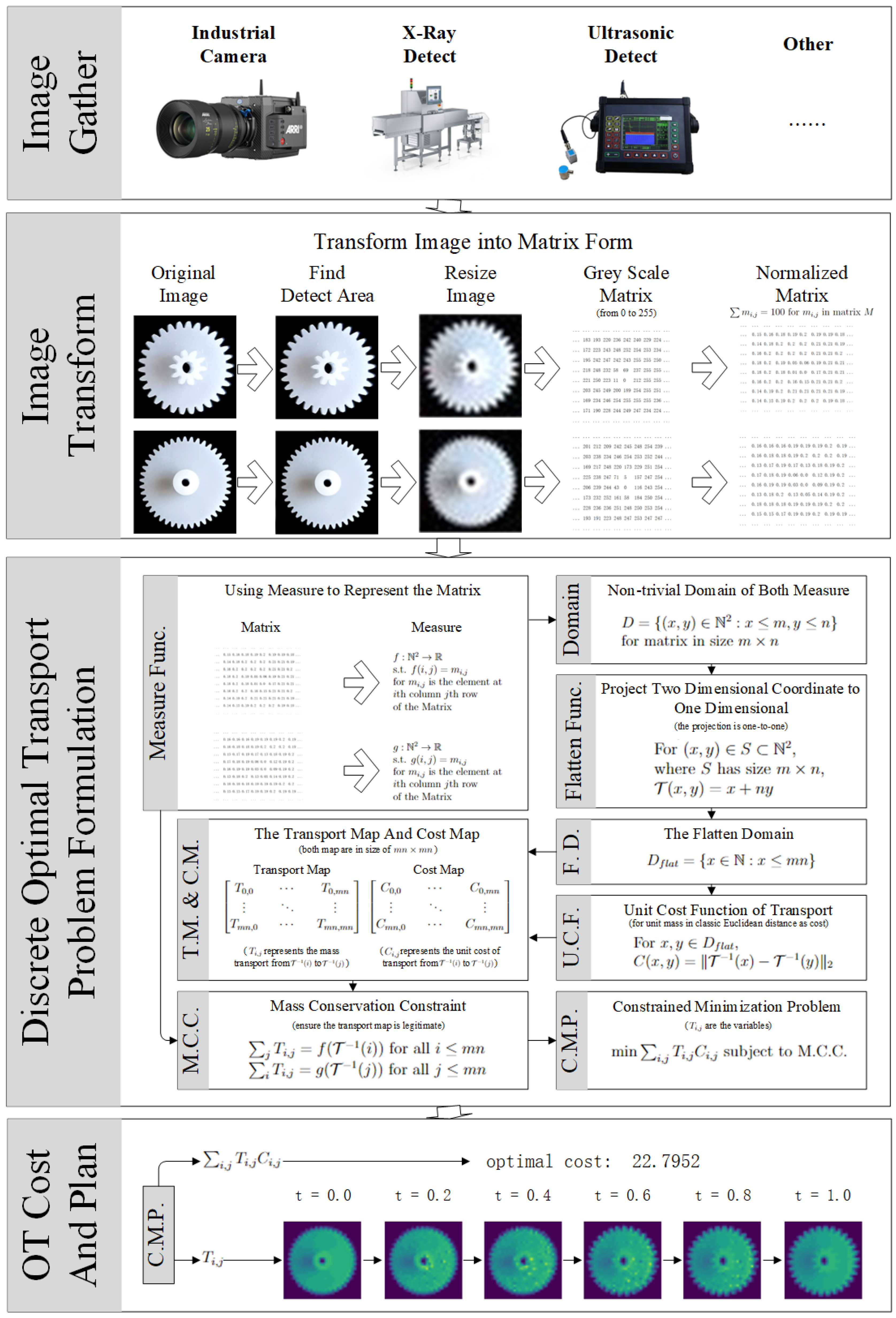
As shown in
Figure 5, we gather two images from various ways and by various equipment. One of them is the detecting image and another is the reference image. Then we find the welding area for the component to detect, and cut both images into the same welding area.
To lower the time consumption, we then resize both images into some convenient size without losing too much precision, and we transform the image into gray scale image. Next, we use matrix to represent every pixel in gray scale image, and we normalize the matrix.
The matrix could be considered as measures over some domain , and we could let Euclidean distance to be the transport cost. By doing so, we form an optimal transport problem. To solve the problem, we project the domain to one dimension, say , by some bijection. Then we formulate the transport map in size of representing how much mass is transport from detecting image to the reference image at each pixel. By such a variable matrix, we then generate a corresponding cost matrix C representing the unit cost for every transport. Flattening the map and cost C, taking dot product would result the cost of transport. Adding constraints of mass conservation, then the optimal transport problem becomes a simple minimizing problem subject to constraints.
By solving the minimization problem, we get the optimal transport map. Using the map, we can have the optimal transport cost, and optimal transport path from detecting image to reference image.
5.2. Image to Matrix
We assume that the input image is in same size as it is assumed in
Section 3.2. We also assume that the input image can be formulated as pixels of some ratio (0-255) of red, green, and blue (RGB). Therefore, an image in RGB can be considered as a matrix where each element is a vector in
. For example:
5.3. Find Welding Area
Since the components on PCB have distinct color in comparison to the color of PCB, we consider matrix
having same size as the RGB matrix such that
contain only R,G,B value in RGB matrix respectively. We define
for
, which represents the average value for elements near the element at
ith row
jth column of matrix
M. Then for the
, say they all have size
, we consider
represents the relative center element of the matrix. Let
be four sets of elements in
R (horizontal, vertical, and diagonal element w.r.t.
c in
R). Let some
such that
, and consider
Define
with same domain as
respectively such that
Let some
to be the threshold that represents the red value range for the component body and the red value for text on it or other color on it if exist. Consider
such that
Then for
, let
to be the values farthest (but connected) from the center of domain which maps to 0 respectively. For rectangle component, we could have the welding area
as follows:
And for component in other shape such as round, we could have the welding area
as follows:
The welding area matrix is defined to be in same shape with R, but every element outside of the welding area is valued by .
Similarly, we take some
, and then we could find two other sets of
for green matrix and blue matrix
. Denoting the welding area of
to be
,
,
respectively. They we say
defined by
to be the welding area.
5.4. Refine Welding Area
Now suppose we have to be the welding areas where is some combination of element in . Since the PCB is in green, we consider function which take the average of elements with non-negative value in jth row and ith column of matrix M, such that the average is defined by for
For each welding area, we could change the value of every element in
ith column to
if
for
is the color range of the PCB. Similarly, we change value at
jth column to
if
Taking (5.6) as an example, the process would be as follows:
5.5. RGB to Normalized Gray Scale
We use the formula
as discussed in [
34] to transform welding area matrix
into gray scale matrix. For example, if we now let the example discussed in
Section 5.2 to be the non-negative part of welding area matrix, we will have the following:
where the element with
is transformed to
Next, we normalize the gray scale matrix where we let the sum of all non-negative element in the matrix to be 100 by letting the element at
ith row
jth column in normalized gray scale matrix to be
where
is the element at
ith row
jth column in gray scale matrix. In this example, we will have the
5.6. Matrix to 2D Measure
While we have a normalized gray scale welding matrix, we can consider the matrix as a space in
where the gray scale value to be the measure on the space. Namely, let
and
To eliminate the unnecessary part and keep only the welding area, we consider
to be the smallest rectangle to contain every element
satisfy
. Consider mapping
that maps
to
. We could then use
to represent the welding area.
With the same example as above subsection, we could have
5.7. Resizing 2D Measure
In order to avoid high computational cost, we could resize the detecting welding area by considering
and
with
for
which takes averages for neighbor measure.
Then we could represent the shrank or resized welding area’s measure by .
5.8. 2D Measure to 1D Measure
As discussed in
Section 4.1, since the element is finite, we can easily construct the flatten function
. Applying
to the space
X, we can get the 1D space
. Assign element
with measure
f on
, denoting as
. Then we have the 1D flat version (
,
) from 2D version (
X,
f).
With the same example as above, we have
, which leads to
5.9. 1D Measure to Discrete OT Problem
Followed by the previous steps, two input images would be transformed into two 1D measures on some
. As discussed in
Section 4.1, we then construct the 1D discrete optimal transport problem as formulated in (
8) and (
9).
If we inherit the example used in previous subsections to be the original image, and we arbitrarily let
to be the 1D measure representing the objective image. Then we will have some transport plans and transport cost as shown in
Table 3 and
Table 4.
Then the discrete optimal transport problem is to find the transport plan that minimizes satisfying the marginal, namely the sum of each column equals to the value above and the sum of each row equals to the value on the left.
5.10. Discrete OT Problem to LP Problem
As discussed in
Section 4.2, we could construct the minimizing problem as in (
13). Followed by the example, we will have
and
5.11. LP Problem Solution to Optimal Cost and Optimal Plan
Solving the LP problem gives argmin, which corresponds to the optimal transport map. Suppose is the solution to the LP problem, then is the optimal transport cost. For , moving amount of mass from to is the optimal transport plan.
For the same example, the solution to the constrained minimization problem is given by
which can be reformulated as in
Table 5.
Applying
to the plan, we finally get the transport plan from measure
f to measure
g.
5.12. Intermediate Images
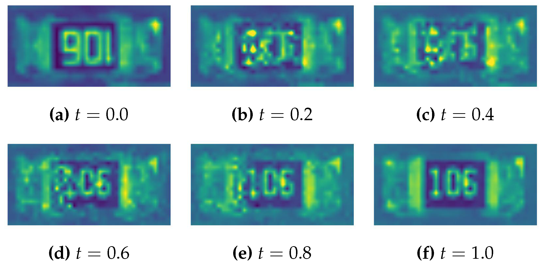
For each assignment, we can consider moving path where is the initial position and is the final position. Then for intermediate status , the mass is located at . For each assignment, finding the closest coordinate add the transporting mass to the position, then subtracting from the initial position would give a intermediate image representing the moving status at time according to the optimal transport plan.
6. Experimental Result and Discussion
The proposed Discrete Optimal Transport Based Welding Defect Detection Method is implemented in Python 3.11.4. The experimental configuration is Intel Core i9-13900K CPU @5.00 GHz with 128 GB memory and RTX 4070 Ti GPU. The test data are gathered from real PCB manufacturing line of intelligent gas meter from Qinchuan IoT Technology Co.,Ltd. In this section, we will show the following advantages of the proposed method from real welding status for components on PCB.
(Precision) Sensitivity to slight change in image
(Efficiency) Computational cost comparison for entire component and only welding part
(Independency) Do not need large training data sets
(Directivity) Can provide actionable insights for manufacturing process improvement and product repair
6.1. Image Gathering
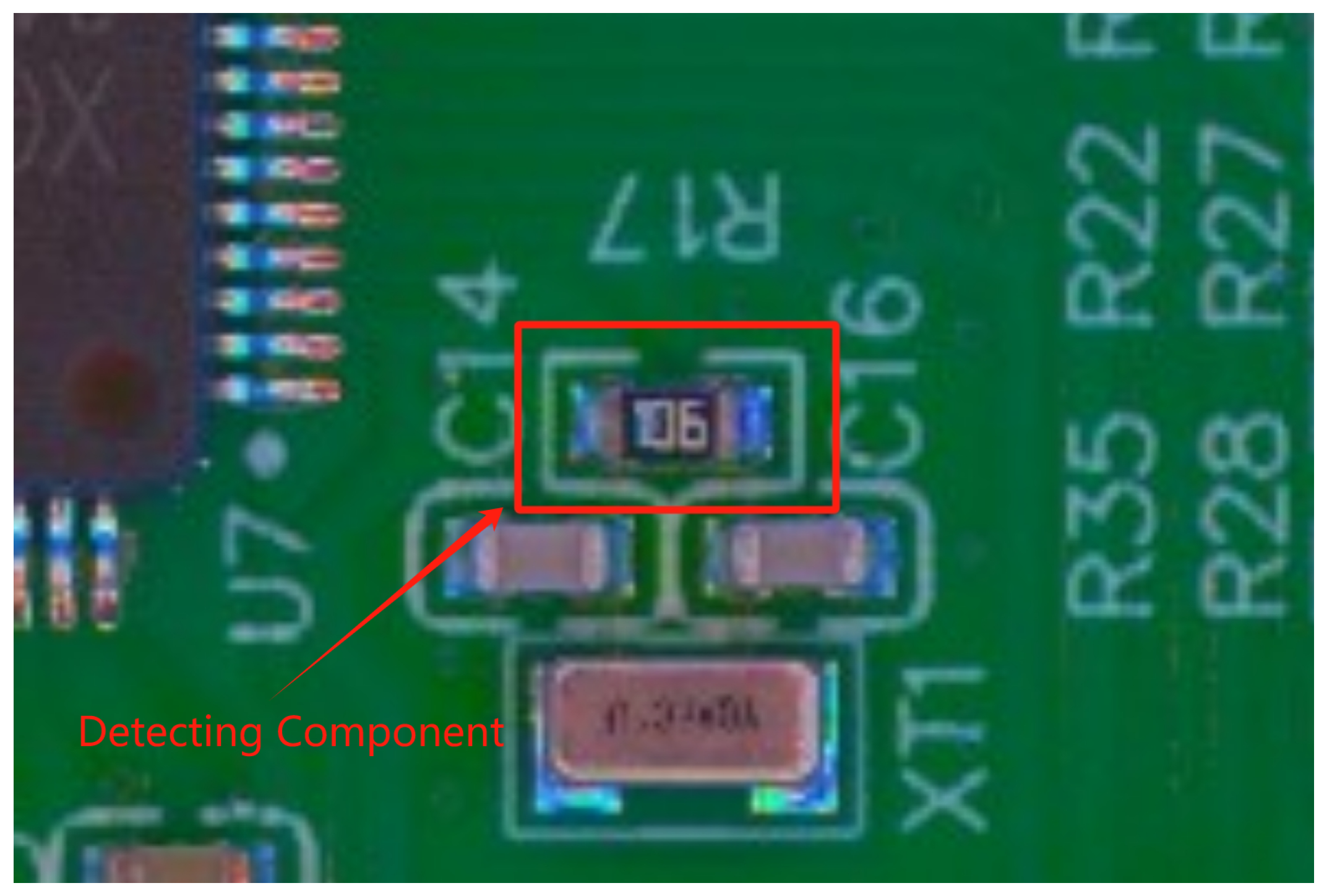
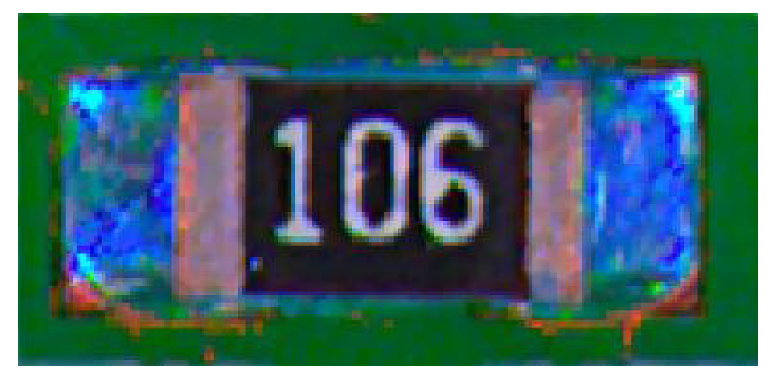
For each PCB manufactured, we take a picture from the above. Since the position of PCB in image stay in some range, and also the component to detect stay in some range in PCB, we can easily get a relative small area containing the component (as shown in
Figure 6).
6.2. Sample And Standard Image
Since for each component, there is a white rectangle-like box containing the component, we can then get the cleaner image of the detecting component by methods such as finding contours. Then we can compare the image (
Figure 7) with the standard image (
Figure 8). Note that the standard image could come from various origin such as previous qualified product, simulation, etc.
6.3. Find Welding Area
Once we obtained the detecting component, we first transform the RGB image into RGB matrix as discussed in
Section 5.2. Since we know the detecting component is in rectangle shape, we then use the Welding Area Finding method discussed in
Section 5.3 with
where taking
to be the farthest value mapped to 0 by
. Then we take
and
to be detecting welding areas (as shown in
Figure 9, the welding areas are L and R). Then, with the same
and
, we also find the detecting welding area for the reference image as follows in
Figure 10.
6.4. Defect Detection
Following the method discussed from
Section 5.4 to 5.12, we could compare the right detecting welding area with the right welding area of the standard image, and for the left welding area, we compare with the left welding area of the standard image.
As shown in the
Table 6,
Table 7 and
Table 8, the practical time complexity of solving optimal transport problem in the proposed method is approximately
. Thus by localizing the welding area, we significantly lower the computational cost with no harm in precision.
Also, the proposed method is extremely sensitive to slight defect. As we can see that the similar welding images in
Figure 7 results in very different optimal transport cost. Any small difference in measure will reflect on the optimal transport plan since the mass change need to be transported out or filled in. This can be illustrated very clearly by
Figure 11,
Figure 12,
Figure 13 and
Figure 14. The difference in detecting welding area will be represented by different measure (or we could consider it as different mass distribution) and to find the optimal transport plan will need to deal with these differences. A small difference could result in different transport plan for a large neighborhood of such a difference.
This can be supported by the
Table 9, where the result in optimal transport cost change is based on changing the gray scale value for some randomly chosen point(s) in the detecting welding area. Note that if the change exceed the min and max of 0 and 255, then the changed value will be limited in the range
Therefore, another advantage of only detecting the welding area is that it could avoid the error due to the pattern or text on detecting component. For example, in
Figure 15 and
Figure 16, the optimal transport plan need to consider the mass for the text printed on the component, even the text is unimportant.
Looking at the optimal cost for same set of samples with different resized size in
Table 6 and
Table 7, we could see that while the resolution of detecting welding area increases 4 times, the optimal cost approximately doubles. This is due to the Euclidean transport cost we chose. It also shows that reasonably resizing the size does not harm precision very much.
Note that the only input data we need is two images: the detecting image and reference image. During the detecting process, there is no outside data used. The welding area finding process, image resizing process, optimal transport problem generating process, etc. are all done locally. The independency on large training data set allow this method to omit the training process and to be applied in data scarce welding defect detecting scene.
Finally, the method not only compare two imagess’ difference, but also gives a path for one image to transform to another. As shown in
Figure 11,
Figure 12,
Figure 13 and
Figure 14, the method unveil the possible way for the detecting welding area to become ideal based on 2D image. It may also help to trace back to potential issues in manufacturing process. For example, if a batch of PCB all has problem on the same component, and the optimal transport path shows the similar mass moving trends, then it is very possible that the welding strategy of the welding machine has issue when dealing with this component. By considering the optimal transport path, the welding machine may add deviation to its strategy based on the path.
7. Conclusions
This study addressed the lack of welding defect detecting method that could maintain precision, be independent to training data, relatively cost low in computation, and guide the potential issue tracing in manufacturing process and the afterwards repair. An welding defect detecting method based on discrete optimal transport was proposed. First, the discrete optimal transport problem based on image comparison was established, and a solver transforming discrete optimal transport problem to linear programming problem was designed to solve the discrete optimal transport problem. Second, a method to process the input detecting image to matrix and then finding the welding area was proposed. In this method, images were transformed into RGB matrix, and by detecting the edges of component, the welding areas were derived from the matrix. Third, a way to transform matrix into 2D measure on was proposed. The welding area is defined in measure and the non-welding area is eliminated from the domain. Fourth, a resizing model is proposed to resize the measure on into smaller domain was proposed. It takes the weighted average over the neighborhood in order to summarize the information. Finally, with the resized 2D measure, the discrete optimal transport problem can be formulated and solved by the solver. According to the optimal transport plan, the transport path from the image of detecting welding area to the image of standard welding area could be generated, as well as the intermediate status.
However, there also exist some limitations for this method. Although the time complexity in practice is not bad, the time consumption remains high when the size of image is large since the variable is the square of total pixels of the image. Considering continuous transport or semi-continuous transport may benefits in some cases. Another limitation is that the method proposed in this paper only analyzes a 2 dimensional image. It is possible that the images of same object are different due to the different position of camera. Using multiple images to form a 3 dimensional density and finding the optimal transport may be the way to solve it.
Funding
This research received no external funding
Institutional Review Board Statement
Not applicable.
Informed Consent Statement
Not applicable.
Data Availability Statement
Acknowledgments
I would like to sincerely thank Professor Weizhi Liao from University of Electronic Science and Technology of China for her guidance and help.
Conflicts of Interest
The author declare no conflicts of interest.
References
- Li, F.; Wu, X.; Phillips, M.A. Technical efficiency of the urban gas industry in china. Environmental Science and Pollution Research 2023, 30, 104477–104488. [Google Scholar] [CrossRef] [PubMed]
- Huang, L. City natural gas metering. Natural Gas—Extraction to End Use; Gupta, SB, Ed.; InTech: Rijeka, Croatia, 2012; pp. 181–208. [Google Scholar]
- Zehua, S. Intertet of Things And Smart City; Renmin Unviersity of China Press, 2022.
- Webster, J.G.; Eren, H. Measurement, Instrumentation, and Sensors Handbook: Two-Volume Set; CRC press, 2018.
- Sun, Q.; Li, H.; Ma, Z.; Wang, C.; Campillo, J.; Zhang, Q.; Wallin, F.; Guo, J. A comprehensive review of smart energy meters in intelligent energy networks. IEEE Internet of Things Journal 2015, 3, 464–479. [Google Scholar] [CrossRef]
- Ilea, P.; Săvescu, D.; Stoica, A. Some aspects of gas meter quality and analyzing the sustainability of a gas meter element. In Proceedings of the IOP Conference Series: Materials Science and Engineering. IOP Publishing, 2019, Vol. 568, p. 012063.
- Wu, R.; Backus, S.; Basu, I.; Blanchard, P.; Brice, K.; Dryfhout-Clark, H.; Fowlie, P.; Hulting, M.; Hites, R. Findings from quality assurance activities in the Integrated Atmospheric Deposition Network. Journal of Environmental Monitoring 2009, 11, 277–296. [Google Scholar] [CrossRef] [PubMed]
- Hacke, P.; Lokanath, S.; Williams, P.; Vasan, A.; Sochor, P.; TamizhMani, G.; Shinohara, H.; Kurtz, S. A status review of photovoltaic power conversion equipment reliability, safety, and quality assurance protocols. Renewable and Sustainable Energy Reviews 2018, 82, 1097–1112. [Google Scholar] [CrossRef]
- Kavitha, R.; Akshatha, K. Component identification and defect detection of printed circuit board using artificial intelligence. In Proceedings of the 2023 2nd International Conference on Applied Artificial Intelligence and Computing (ICAAIC). IEEE. 2023; pp. 100–106. [Google Scholar]
- Sezer, A.; Altan, A. Optimization of deep learning model parameters in classification of solder paste defects. In Proceedings of the 2021 3rd international congress on human-computer interaction, optimization and robotic applications (HORA). IEEE. 2021; pp. 1–6. [Google Scholar]
- Chen, I.C.; Hwang, R.C.; Huang, H.C. Pcb defect detection based on deep learning algorithm. Processes 2023, 11, 775. [Google Scholar] [CrossRef]
- Chen, X.; Wu, Y.; He, X.; Ming, W. A comprehensive review of deep learning-based PCB defect detection. IEEE Access 2023. [Google Scholar] [CrossRef]
- Ling, Q.; Isa, N.A.M. Printed circuit board defect detection methods based on image processing, machine learning and deep learning: A survey. IEEE Access 2023, 11, 15921–15944. [Google Scholar] [CrossRef]
- Baygin, M.; Karakose, M.; Sarimaden, A.; Erhan, A. Machine vision based defect detection approach using image processing. In Proceedings of the 2017 international artificial intelligence and data processing symposium (IDAP). Ieee. 2017; pp. 1–5. [Google Scholar]
- Chang, Y.; Xue, Y.; Zhang, Y.; Ma, J.; Li, G.; Wu, D.; Zhan, Q.; Zuo, J. Research on PCB solder joint defect detection method based on machine vision. In Proceedings of the Fourteenth International Conference on Graphics and Image Processing (ICGIP 2022). SPIE, 2023. Vol. 12705; pp. 181–188.
- Bhatt, P.M.; Malhan, R.K.; Rajendran, P.; Shah, B.C.; Thakar, S.; Yoon, Y.J.; Gupta, S.K. Image-based surface defect detection using deep learning: A review. Journal of Computing and Information Science in Engineering 2021, 21, 040801. [Google Scholar] [CrossRef]
- Liu, G. Surface defect detection methods based on deep learning: a brief review. In Proceedings of the 2020 2nd International Conference on Information Technology and Computer Application (ITCA). IEEE. 2020; pp. 200–203. [Google Scholar]
- Kantorovich, L.V. On the Translocation of Masses. Journal of mathematical sciences 2006, 133. [Google Scholar] [CrossRef]
- Liu, Z.; Qu, B. Machine vision based online detection of PCB defect. Microprocessors and Microsystems 2021, 82, 103807. [Google Scholar] [CrossRef]
- Ren, Z.; Fang, F.; Yan, N.; Wu, Y. State of the art in defect detection based on machine vision. International Journal of Precision Engineering and Manufacturing-Green Technology 2022, 9, 661–691. [Google Scholar] [CrossRef]
- Liao, S.; Huang, C.; Zhang, H.; Gong, J.; Li, M.; Wang, Z. Object detection of welding defects in SMT electronics production based on deep learning. In Proceedings of the 2022 23rd International Conference on Electronic Packaging Technology (ICEPT). IEEE, 2022. pp. 1–5.
- Legon, A.; Deo, M.; Albin, S.; Audette, M. Detection and classification of PCB defects using deep learning methods. In Proceedings of the 2022 IEEE 31st Microelectronics Design & Test Symposium (MDTS). IEEE, 2022. pp. 1–6.
- Liu, X.; Wang, J.; Zhang, R.; Ruan, W. Deep learning-based defect detection for printed circuit boards. In Proceedings of the Third International Conference on Computer Vision and Pattern Analysis (ICCPA 2023). SPIE, 2023. Vol. 12754; pp. 897–902.
- Ling, Z.; Zhang, A.; Ma, D.; Shi, Y.; Wen, H. Deep Siamese semantic segmentation network for PCB welding defect detection. IEEE Transactions on Instrumentation and Measurement 2022, 71, 1–11. [Google Scholar] [CrossRef]
- Pham, T.T.A.; Thoi, D.K.T.; Choi, H.; Park, S. Defect detection in printed circuit boards using semi-supervised learning. Sensors 2023, 23, 3246. [Google Scholar] [CrossRef] [PubMed]
- Mémoli, F. Gromov–Wasserstein distances and the metric approach to object matching. Foundations of computational mathematics 2011, 11, 417–487. [Google Scholar] [CrossRef]
- Colombo, M.; Di Marino, S. Equality between Monge and Kantorovich multimarginal problems with Coulomb cost. Annali di Matematica Pura ed Applicata (1923-) 2015, 194, 307–320. [Google Scholar] [CrossRef]
- Dantzig, G.B. Linear programming and extensions. In Linear programming and extensions; Princeton university press, 2016.
- Kuhn, H.W. The Hungarian method for the assignment problem. Naval research logistics quarterly 1955, 2, 83–97. [Google Scholar] [CrossRef]
- Bertsekas, D.P. The auction algorithm: A distributed relaxation method for the assignment problem. Annals of operations research 1988, 14, 105–123. [Google Scholar] [CrossRef]
- Evans, L.C. Partial differential equations and Monge-Kantorovich mass transfer. Current developments in mathematics 1997, 1997, 65–126. [Google Scholar] [CrossRef]
- Banciu, M. Dual simplex. In Wiley Encyclopedia of Operations Research and Management Science; Wiley, 2011.
- Potra, F.A.; Wright, S.J. Interior-point methods. Journal of computational and applied mathematics 2000, 124, 281–302. [Google Scholar] [CrossRef]
- Alrubaie, S.H.; Hameed, A.H. Dynamic weights equations for converting grayscale image to RGB image. Journal of University of Babylon for Pure and Applied Sciences 2018, 26, 122–129. [Google Scholar] [CrossRef]
Figure 1.
Given two terrains defined as probability density , where represented as gray scale here, Monge’s problem is to minimize the cost of transforming the terrain represented by f into terrain represented by g. The transport plan T need to satisfy the mass conservation constraint, where any random portion in density g must be transported from some portion with same mass in density f.
Figure 2.
For any transport plan to transport f to , there exist better plan by splitting f into twice more pieces. So that there exist no optimal transport plan. This is since transport plan T cannot send same point, say x, to two different places, say .
Figure 2.
For any transport plan to transport f to , there exist better plan by splitting f into twice more pieces. So that there exist no optimal transport plan. This is since transport plan T cannot send same point, say x, to two different places, say .
Figure 3.
Kantorovitch’s Relaxed Problem Example
Figure 3.
Kantorovitch’s Relaxed Problem Example
Figure 4.
One Dimensional Discrete Optimal Transport Problem Example
Figure 4.
One Dimensional Discrete Optimal Transport Problem Example
Figure 6.
The Detecting Component
Figure 6.
The Detecting Component
Figure 9.
Welding Area of Sample 3
Figure 9.
Welding Area of Sample 3
Figure 10.
Welding Area of Standard Image
Figure 10.
Welding Area of Standard Image
Figure 11.
Left Part Comparison of Sample 3 (Optimal Cost: 56.70).
Figure 11.
Left Part Comparison of Sample 3 (Optimal Cost: 56.70).
Figure 12.
Right Part Comparison of Sample 3 (Optimal Cost: 69.93).
Figure 12.
Right Part Comparison of Sample 3 (Optimal Cost: 69.93).
Figure 13.
Left Part Comparison of Sample 7 (Optimal Cost: 146.81).
Figure 13.
Left Part Comparison of Sample 7 (Optimal Cost: 146.81).
Figure 14.
Right Part Comparison of Sample 7 (Optimal Cost: 57.54).
Figure 14.
Right Part Comparison of Sample 7 (Optimal Cost: 57.54).
Figure 15.
Sample 1 in Defect Detect For Single Component (Optimal Cost: 55.71).
Figure 15.
Sample 1 in Defect Detect For Single Component (Optimal Cost: 55.71).
Figure 16.
Sample 7 in Defect Detect For Single Component (Optimal Cost: 66.03).
Figure 16.
Sample 7 in Defect Detect For Single Component (Optimal Cost: 66.03).
Table 3.
Transport Plan.
| |
|
|
|
|
|
|
|
|
|
|
|
|
|
|
|
|
|
|
|
|
|
|
|
|
Table 4.
Transport Cost (Euclidean Distance).
Table 4.
Transport Cost (Euclidean Distance).
| |
0 |
1 |
2 |
3 |
| 0 |
|
|
|
|
| 1 |
|
|
|
|
| 2 |
|
|
|
|
| 3 |
|
|
|
|
Table 5.
Optimal Transport Plan (Optimal Cost: 35.7679).
Table 5.
Optimal Transport Plan (Optimal Cost: 35.7679).
| |
|
|
|
|
|
20 |
0 |
0 |
|
|
0 |
10 |
0 |
|
|
0 |
0 |
30 |
|
|
0 |
0 |
0 |
|
Table 6.
OT with Size (39,28).
Table 6.
OT with Size (39,28).
| Sample |
Optimal Cost |
Time Cost (s) |
| 1 left |
124.6884 |
81.7439 |
| 1 Right |
42.0153 |
65.8820 |
| 2 left |
97.4181 |
70.4414 |
| 2 Right |
90.3658 |
66.4491 |
| 3 left |
56.7008 |
54.8580 |
| 3 Right |
69.9283 |
76.9399 |
| 4 left |
89.5546 |
75.1159 |
| 4 Right |
72.1899 |
67.7810 |
| 5 left |
51.8627 |
74.7324 |
| 5 Right |
59.4787 |
58.4266 |
| 6 left |
72.9623 |
79.0964 |
| 6 Right |
105.3368 |
88.5780 |
| 7 left |
146.8131 |
76.0858 |
| 7 Right |
57.5372 |
64.3336 |
| 8 left |
110.2959 |
57.8042 |
| 8 Right |
52.8154 |
73.2075 |
| 9 left |
90.6085 |
71.9530 |
| 9 Right |
59.2622 |
80.9185 |
| 10 left |
76.7273 |
65.0734 |
| 10 Right |
91.0504 |
79.3705 |
Table 7.
OT with Size (19,14).
Table 7.
OT with Size (19,14).
| Sample |
Optimal Cost |
Time Cost (s) |
| 1 left |
61.8171 |
1.0307 |
| 1 Right |
21.8712 |
0.9719 |
| 2 left |
47.5094 |
1.0532 |
| 2 Right |
46.5524 |
1.0328 |
| 3 left |
29.6239 |
0.9313 |
| 3 Right |
31.6513 |
1.0388 |
| 4 left |
42.4647 |
1.0107 |
| 4 Right |
32.1805 |
0.9507 |
| 5 left |
24.3411 |
1.0018 |
| 5 Right |
29.5494 |
0.9604 |
| 6 left |
36.7987 |
0.9448 |
| 6 Right |
53.9450 |
1.0180 |
| 7 left |
72.1791 |
1.0598 |
| 7 Right |
30.2502 |
0.9749 |
| 8 left |
56.6340 |
0.9490 |
| 8 Right |
27.3963 |
1.0443 |
| 9 left |
43.7873 |
0.9613 |
| 9 Right |
32.8113 |
1.0480 |
| 10 left |
39.7919 |
0.9684 |
| 10 Right |
44.2695 |
1.0034 |
Table 8.
Optimal Transport for Entire Component with Size (19,38).
Table 8.
Optimal Transport for Entire Component with Size (19,38).
| Sample |
Time Consumption (s) |
| 1 |
14.2441 |
| 2 |
13.8762 |
| 3 |
14.1679 |
| 4 |
14.6666 |
| 5 |
14.1432 |
| 6 |
14.0194 |
| 7 |
14.2059 |
| 8 |
14.1208 |
| 9 |
13.7494 |
| 10 |
13.9204 |
Table 9.
Sensitivity in Optimal Transport with Size (19,14): Using the Transport from Sample 3 to the Standard As Example.
Table 9.
Sensitivity in Optimal Transport with Size (19,14): Using the Transport from Sample 3 to the Standard As Example.
| Pixel Changed |
Value Changed |
Cost Changed |
| (7,0) |
+1 |
-0.0059 |
| |
+5 |
-0.0297 |
| |
+10 |
-0.0585 |
| |
+20 |
-0.1151 |
| (3,13) |
+1 |
-0.0072 |
| |
+5 |
-0.0357 |
| |
+10 |
-0.0708 |
| |
+20 |
-0.1136 |
| (8,10) |
+1 |
+0.0048 |
| |
+5 |
+0.0242 |
| |
+10 |
+0.0486 |
| |
+20 |
+0.1090 |
|
Disclaimer/Publisher’s Note: The statements, opinions and data contained in all publications are solely those of the individual author(s) and contributor(s) and not of MDPI and/or the editor(s). MDPI and/or the editor(s) disclaim responsibility for any injury to people or property resulting from any ideas, methods, instructions or products referred to in the content. |
© 2024 by the authors. Licensee MDPI, Basel, Switzerland. This article is an open access article distributed under the terms and conditions of the Creative Commons Attribution (CC BY) license (http://creativecommons.org/licenses/by/4.0/).

