
Submitted:
12 December 2024
Posted:
13 December 2024
You are already at the latest version
Abstract
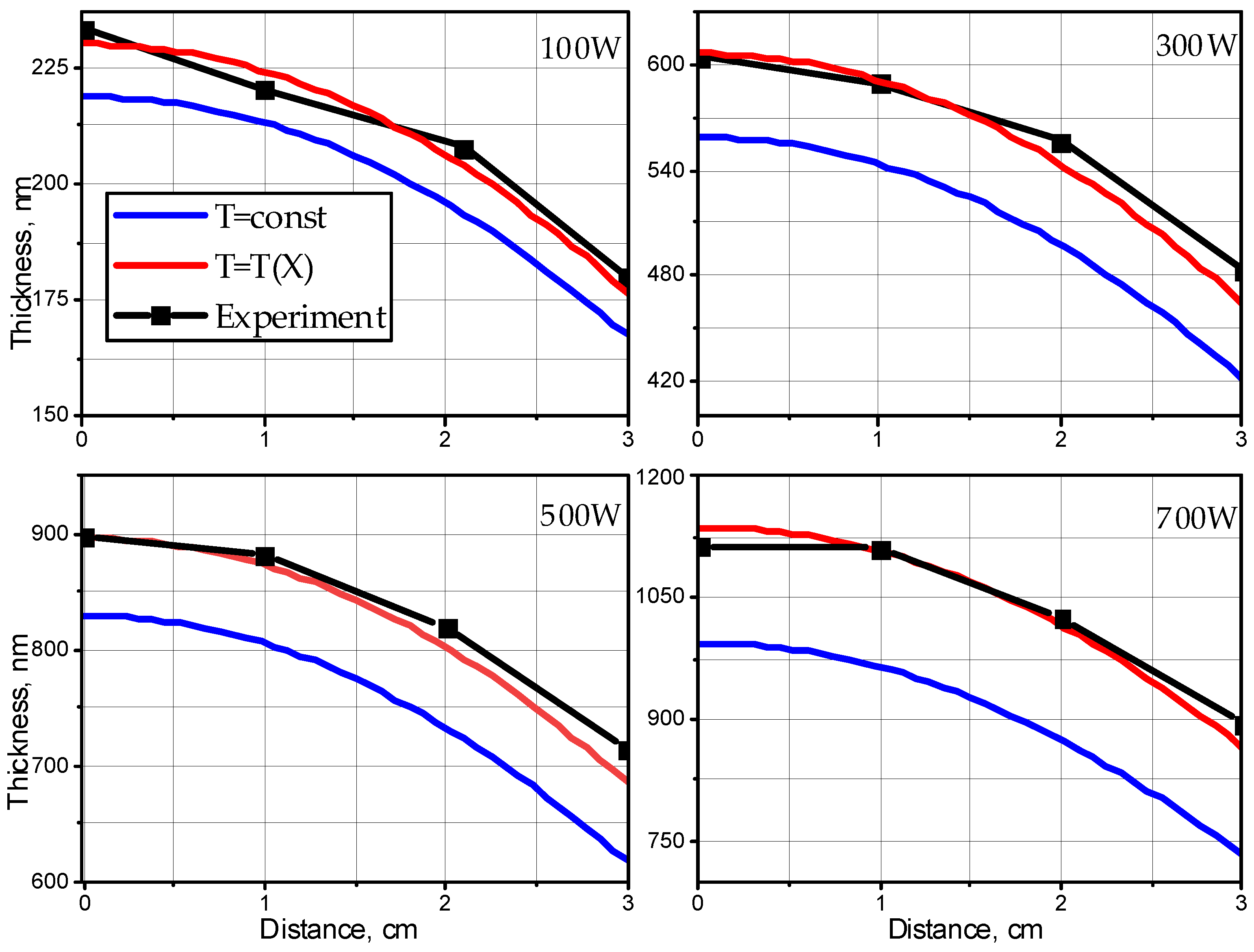
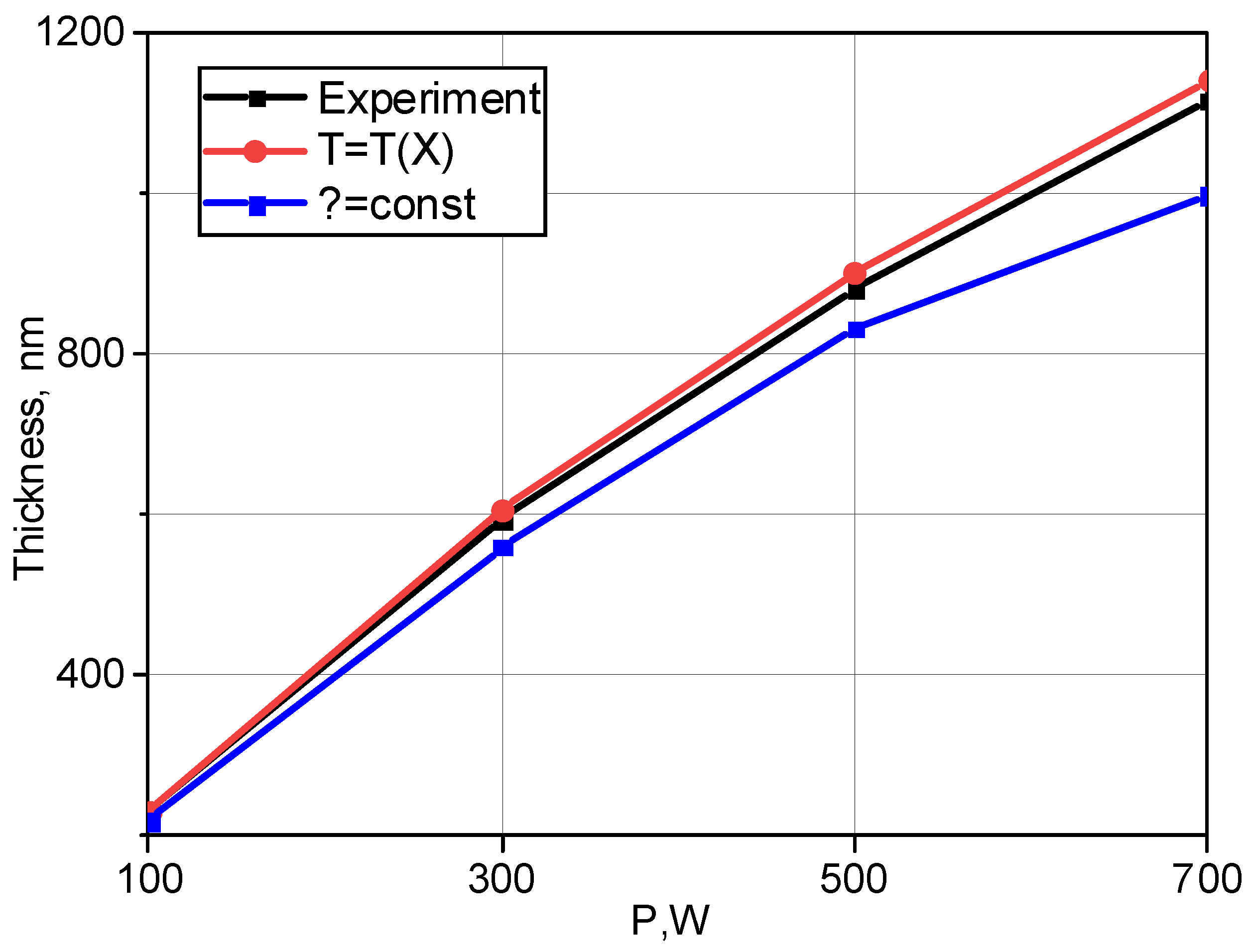
A theoretical model is proposed that allows us to describe the processes of formation of the sputtered atom flow, transport of this flow in the target-substrate space and deposition of the substance onto the substrate during magnetron sputtering. The main difference between the presented model and the existing ones is the combined consideration of the spatial distribution of sputtered atoms and the temperature gradient in the working chamber during magnetron sputtering at high power. To verify the model, real technological parameters of deposition of metal films by magnetron sputtering were used, optimized to achieve a high film growth rate. The agreement between the calculated film thicknesses obtained as a result of modeling and the experimental data was no worse than 5% at discharge powers in the range of 100 – 700 W. Comparison of the experimental data with the simulation results showed that the model adequately describes the sputtering processes at high discharge powers and low pressures, in contrast to approaches that do not take into account the temperature gradient in the working space.
Keywords:
1. Introduction
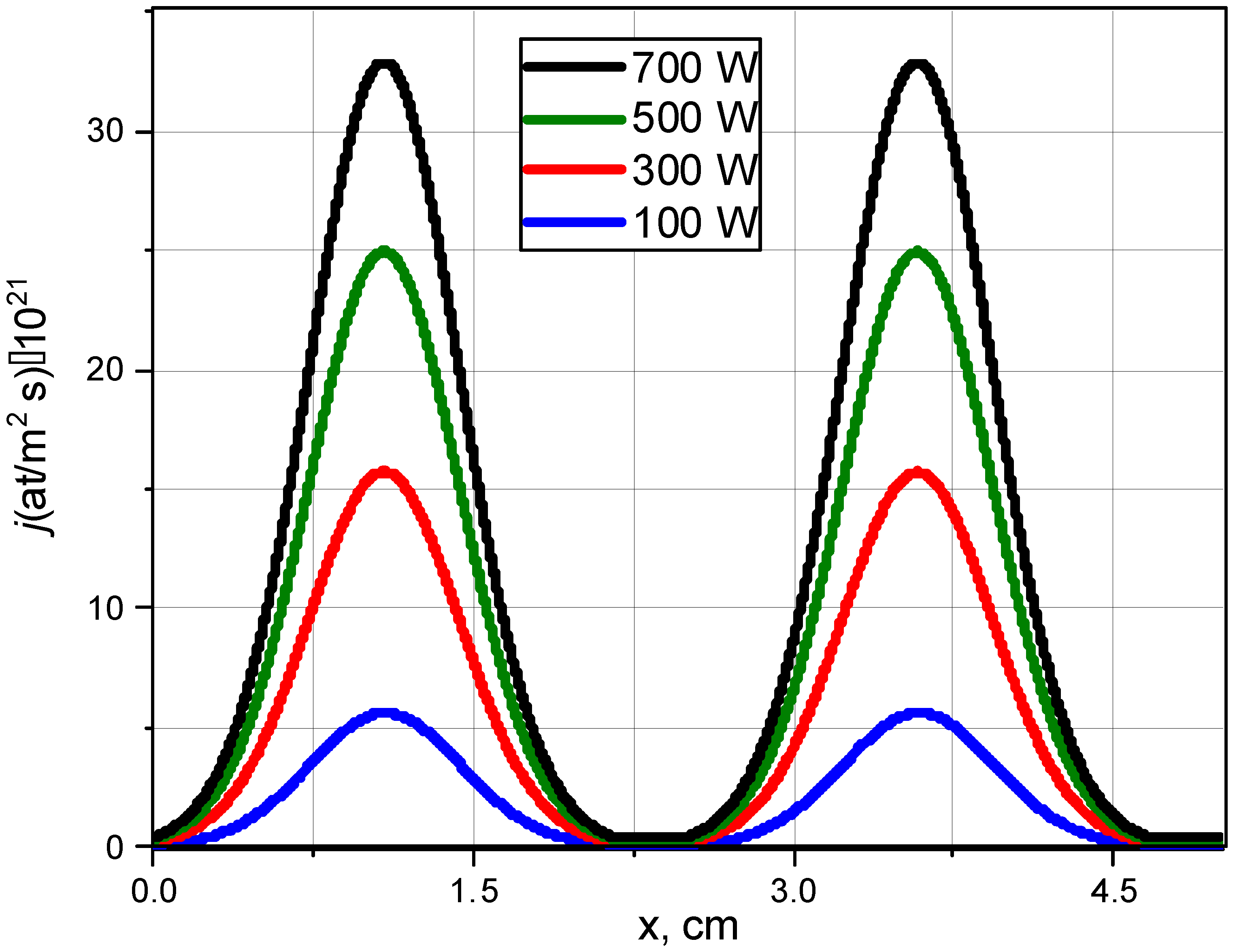
2. Experiment
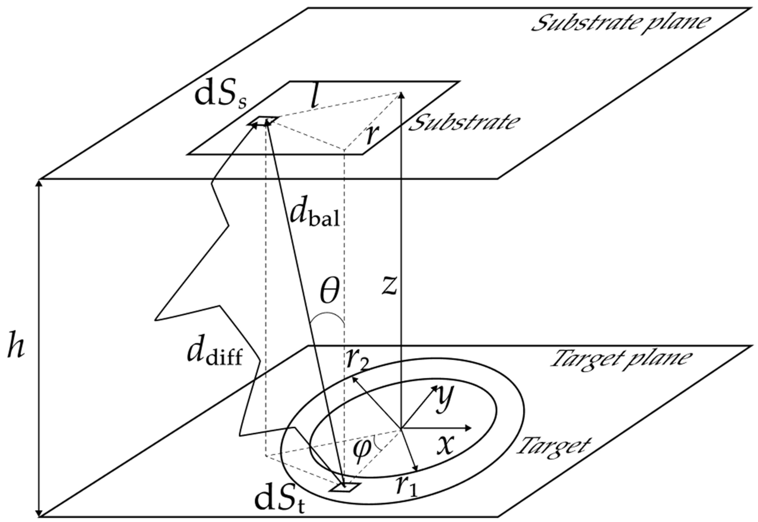
3. Description of the Model
3.1. Target Sputtering
3.2. Transfer of Working Substance
3.3. Deposition of the Working Substance on the Substrate
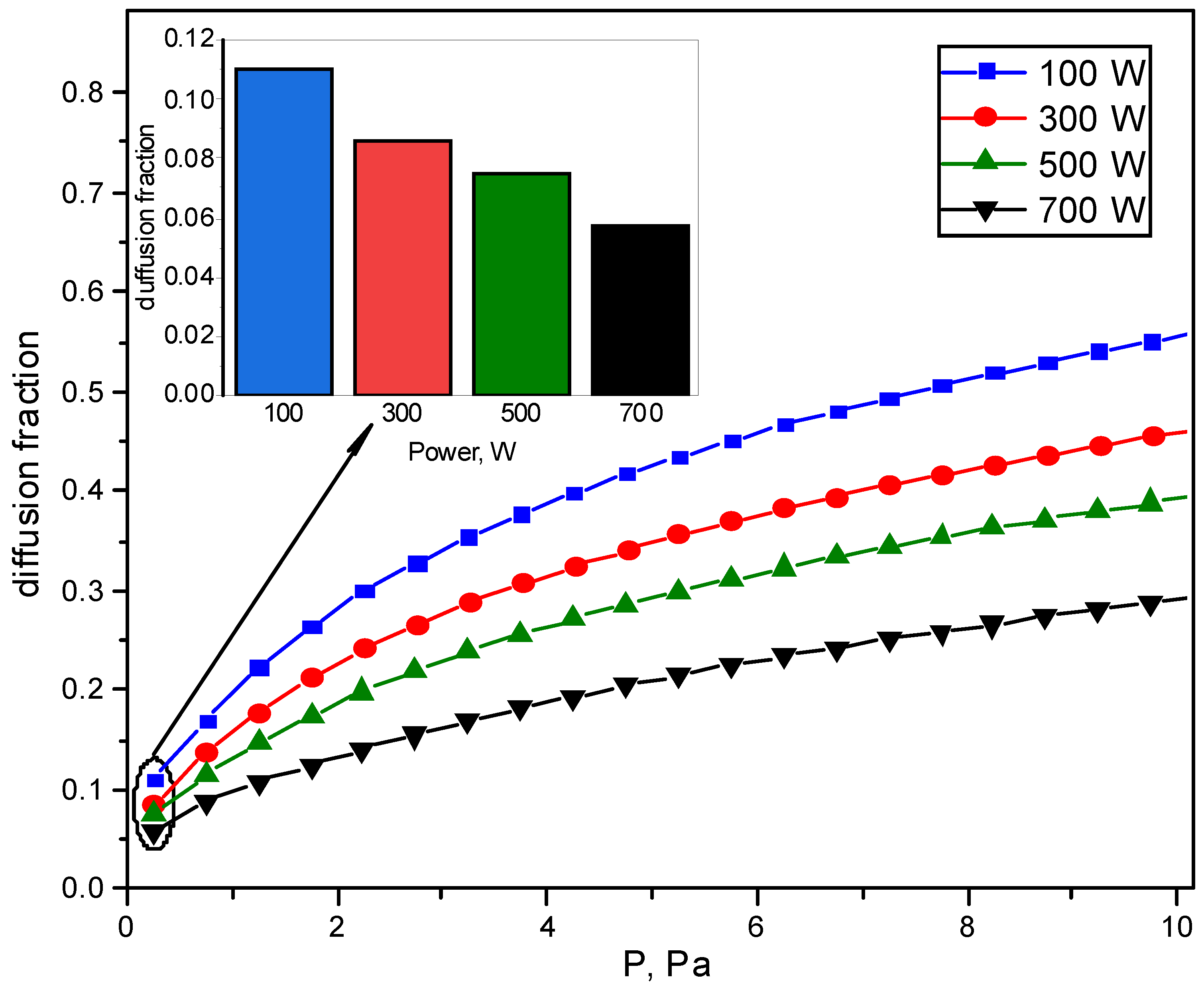
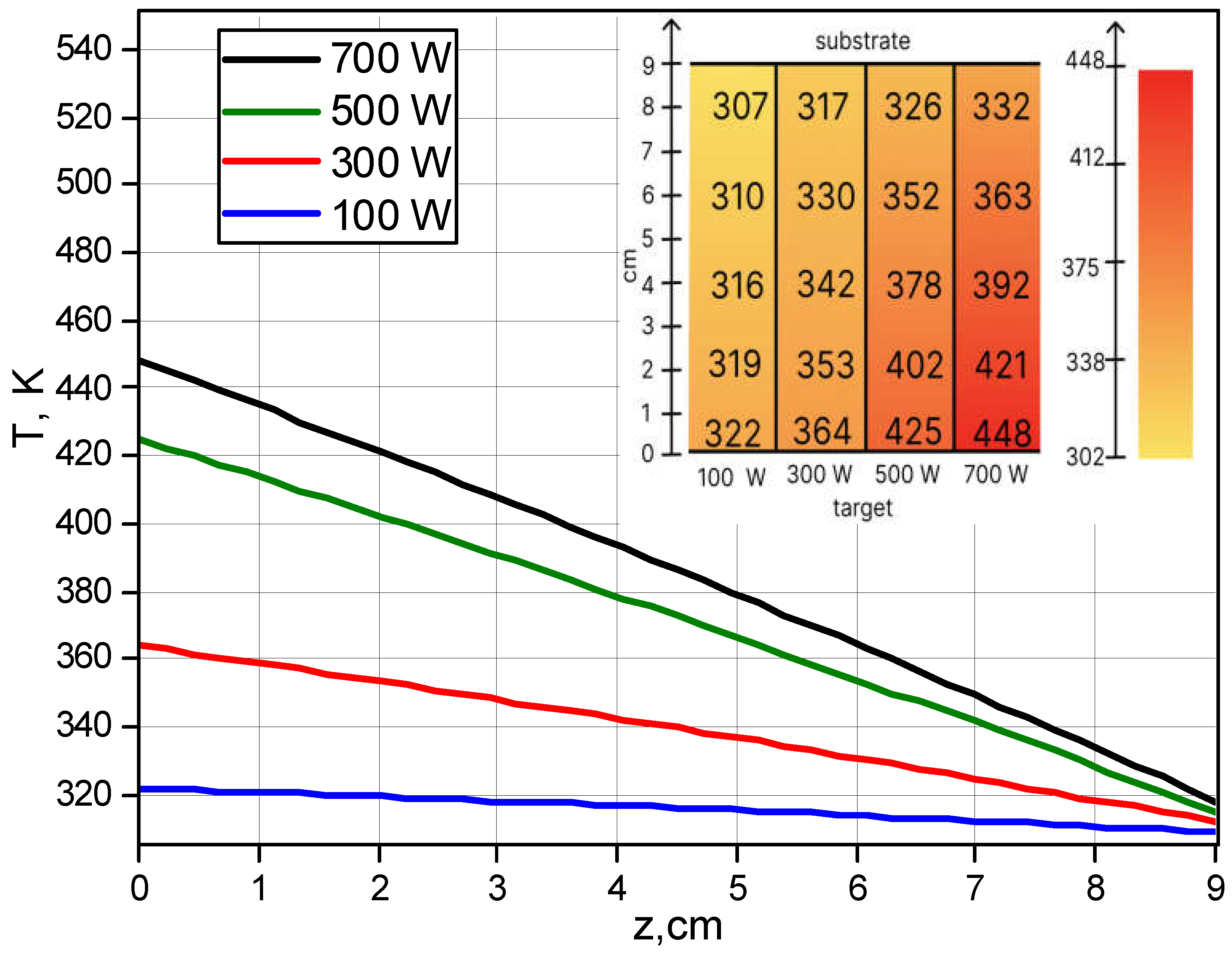
4. Results and Discussion
5. Conclusions
Author Contributions
Funding
Data Availability Statement
Conflicts of Interest
References
- Alfonso, E.; Olaya, J.; Cubillos, G. Thin Film Growth Through Sputtering Technique and Its Applications. In Crystallization - Science and Technology; Andreeta, M., Ed.; Rijeka Croatia, 2012; pp. 10–21. [Google Scholar] [CrossRef]
- Rossnagel, S.M. Magnetron Sputtering. Journal of Vacuum Science & Technology A: Vacuum, Surfaces, and Films 2020, 38, 060805. [Google Scholar] [CrossRef]
- Gudmundsson, J.T.; Lundin, D. Introduction to magnetron sputtering; Elsevier, 2020; pp. 1–48. [Google Scholar] [CrossRef]
- Anders, A. Tutorial: Reactive High Power Impulse Magnetron Sputtering (R-HiPIMS). Journal of Applied Physics, 2017; 121, 171101. [Google Scholar] [CrossRef]
- Baptista, A.; Silva, F.J.G.; Porteiro, J.; Míguez, J.L.; Pinto, G.; Fernandes, L. On the Physical Vapour Deposition (PVD): Evolution of Magnetron Sputtering Processes for Industrial Applications. Procedia Manufacturing 2018, 17, 746–757. [Google Scholar] [CrossRef]
- Jeyachandran, Y.L.; Karunagaran, B.; Narayandass, Sa.K.; Mangalaraj, D.; Jenkins, T.E.; Martin, P.J. Properties of Titanium Thin Films Deposited by Dc Magnetron Sputtering. Materials Science and Engineering: A 2006, 431, 277–284. [Google Scholar] [CrossRef]
- Muralidhar Singh, M.; Vijaya, G.; Krupashankara, M.S.; Sridhara, B.K.; Shridhar, T.N. Deposition and Characterization of Aluminium Thin Film Coatings Using DC Magnetron Sputtering Process. Materials Today: Proceedings 2018, 5, 2696–2704. [Google Scholar] [CrossRef]
- Wang, S.-F.; Lin, H.-C.; Bor, H.-Y.; Tsai, Y.-L.; Wei, C.-N. Characterization of Chromium Thin Films by Sputter Deposition. Journal of Alloys and Compounds 2011, 509, 10110–10114. [Google Scholar] [CrossRef]
- Depla, D.; Tomaszewski, H.; Buyle, G.; De Gryse, R. Influence of the Target Composition on the Discharge Voltage during Magnetron Sputtering. Surface and Coatings Technology 2006, 201, 848–854. [Google Scholar] [CrossRef]
- Ahmed, N.; Iqbal, M.A.; Khan, Z.S.; Qayyum, A.A. DC Magnetron-Sputtered Mo Thin Films with High Adhesion, Conductivity and Reflectance. Journal of Electronic Materials 2020, 49, 4221–4230. [Google Scholar] [CrossRef]
- Paturaud, C.; Farges, G.; Sainte Catherine, M.C.; Machet, J. Influence of Sputtering Gases on the Properties of Magnetron Sputtered Tungsten Films. Surface and Coatings Technology 1996, 86-87, 388–393. [Google Scholar] [CrossRef]
- Thaveedeetrakul, A.; Witit-anun, N.; Boonamnuayvitaya, V. The Role of Target-to-Substrate Distance on the DC Magnetron Sputtered Zirconia Thin Films’ Bioactivity. Applied Surface Science 2012, 258, 2612–2619. [Google Scholar] [CrossRef]
- Gudmundsson, J.T. Physics and technology of magnetron sputtering discharges. Plasma Sources Science and Technology 2020, 29, 113001. [Google Scholar] [CrossRef]
- Sheridan, T.E.; Goeckner, M.J.; Goree, J. Model of Energetic Electron Transport in Magnetron Discharges. Journal of Vacuum Science & Technology A: Vacuum, Surfaces, and Films 1990, 8, 30–37. [Google Scholar] [CrossRef]
- Kaziev, A.V. Cathode Sheath Processes in a Non-Sputtering Magnetron Discharge. Vacuum 2018, 158, 191–194. [Google Scholar] [CrossRef]
- Thornton, J.A. Magnetron sputtering: basic physics and application to cylindrical magnetrons. Journal of Vacuum Science and Technology 1978, 15, 171–177. [Google Scholar] [CrossRef]
- Westwood, W.D.; Maniv, S.; Scanlon, P.J. The Current-Voltage Characteristic of Magnetron Sputtering Systems. Journal of Applied Physics 1983, 54, 6841–6846. [Google Scholar] [CrossRef]
- Tumarkin, A.V.; Al’myashev, V.I.; Razumov, S.V.; Gaidukov, M.M.; Gagarin, A.G.; Altynnikov, A.G.; Kozyrev, A.B. Structural Properties of Barium Strontium Titanate Films Grown under Different Technological Conditions. Phys. Solid State 2015, 57, 553–557. [Google Scholar] [CrossRef]
- Lapshin, A.E.; Levitskii, V.S.; Shapovalov, V.I.; Komlev, A.E.; Shutova, E.S.; Myl’nikov, I.L.; Komlev, A.A. Composition and Structure of Copper Oxide Films Synthesized by Reactive Magnetron Sputtering with a Hot Target. Glass Physics Chemistry 2016, 42, 359–362. [Google Scholar] [CrossRef]
- Tan, X.-Q.; Liu, J.-Y.; Niu, J.-R.; Liu, J.-Y.; Tian, J.-Y. Recent Progress in Magnetron Sputtering Technology Used on Fabrics. Materials 2018, 11, 1953. [Google Scholar] [CrossRef]
- Sergievskaya, A.; Chauvin, A.; Konstantinidis, S. Sputtering onto Liquids: A Critical Review. Beilstein J. Nanotechnology 2022, 13, 10–53. [Google Scholar] [CrossRef] [PubMed]
- Sigmund, P. Theory of Sputtering. I. Sputtering Yield of Amorphous and Polycrystalline Targets. Physical Review 1969, 187, 768–768. [Google Scholar] [CrossRef]
- Behrisch, R. Sputtering by particle bombardment. In Sputtering by Particle Bombardment I; Behrisch, R., Ed.; Topics in Applied Physics; Springer: Berlin, Heidelberg, 1981; Volume 47, pp. 9–71. [Google Scholar]
- Depla, D. On the Effective Sputter Yield during Magnetron Sputter Deposition. Nuclear Instruments and Methods in Physics Research Section B: Beam Interactions with Materials and Atoms 2014, 328, 65–69. [Google Scholar] [CrossRef]
- Gras-Marti, A.; Vallés-Abarca, J.A.; Bensaoula, A. Energy and Momentum Transport by Sputtered and Reflected Streams in a Glow Discharge. Journal of Vacuum Science & Technology A: Vacuum, Surfaces, and Films 1987, 5, 2217–2221. [Google Scholar] [CrossRef]
- Turner, G.M.; Sikorski, A.; McKenzie, D.R.; Smith, G.B.; Ng, K.; Cockayne, D.J.H. Spatial Variations in the Stoichiometry of Sputtered YBaCuO Thin Films: Theory and Experiment. Physica C: Superconductivity 1990, 170, 473–480. [Google Scholar] [CrossRef]
- Petrov, I.; Ivanov, I.; Orlinov, V.; Sundgren, J.-E. Comparison of Magnetron Sputter Deposition Conditions in Neon, Argon, Krypton, and Xenon Discharges. Journal of Vacuum Science & Technology A: Vacuum, Surfaces, and Films 1993, 11, 2733–2741. [Google Scholar] [CrossRef]
- Jakas, M.M. Transport Theories of Sputtering. Philosophical Transactions of the Royal Society of London. Series A: Mathematical, Physical and Engineering Sciences 2004, 362, 139–156. [Google Scholar] [CrossRef]
- Ekpe, S.D.; Dew, S.K. Theoretical and Experimental Determination of the Energy Flux during Magnetron Sputter Deposition onto an Unbiased Substrate. Journal of Vacuum Science & Technology A: Vacuum, Surfaces, and Films 2003, 21, 476–483. [Google Scholar] [CrossRef]
- Zhang, Y.; Song, Q.; Sun, Z. Research on Thin Film Thickness Uniformity for Deposition of Rectangular Planar Sputtering Target. Physics Procedia 2012, 32, 903–913. [Google Scholar] [CrossRef]
- Revel, A.; Farsy, A.E.; De Poucques, L.; Robert, J.; Minea, T. Transition from Ballistic to Thermalized Transport of Metal-Sputtered Species in a DC Magnetron. Plasma Sources Science and Technology 2021, 30, 125005. [Google Scholar] [CrossRef]
- Volpyas, V.A.; Kozyrev, A.B. Thermalization of atomic particles in gases. Journal of Experimental and Theoretical Physics 2011, 113. [Google Scholar] [CrossRef]
- Ekpe, S.D.; Bezuidenhout, L.W.; Dew, S.K. Deposition Rate Model of Magnetron Sputtered Particles. Thin Solid Films 2005, 474, 330–336. [Google Scholar] [CrossRef]
- Hong, S.; Kim, E.; Bae, B.-S.; No, K.; Lim, S.-C.; Woo, S.-G.; Koh, Y.-B. A Simulation Model for Thickness Profile of the Film Deposited Using Planar Circular Type Magnetron Sputtering Sources. Journal of Vacuum Science & Technology A: Vacuum, Surfaces, and Films 1996, 14, 2721–2727. [Google Scholar] [CrossRef]
- Yamamura, Y.; Takiguchi, T.; Ishida, M. Energy and Angular Distributions of Sputtered Atoms at Normal Incidence. Radiation Effects and Defects in Solids 1991, 118, 237–261. [Google Scholar] [CrossRef]
- Ekpe, S.D.; Dew, S.K. 3D Numerical Simulation of Gas Heating Effects in a Magnetron Sputter Deposition System. Journal of Physics D: Applied Physics 2006, 39, 1413–1421. [Google Scholar] [CrossRef]
- Palmero, A.; Rudolph, H.; Habraken, F.H.P.M. Study of the Gas Rarefaction Phenomenon in a Magnetron Sputtering System. Thin Solid Films 2006, 515, 631–635. [Google Scholar] [CrossRef]
- Jimenez, F.; Ekpe, S.D.; Dew, S.K. Inhomogeneous Rarefaction of the Process Gas in a Direct Current Magnetron Sputtering System. Journal of Vacuum Science & Technology A: Vacuum, Surfaces, and Films 2006, 24, 1530–1534. [Google Scholar] [CrossRef]
- Sheikin, E.G. The Pressure Dependence of the Deposition Rate in a Magnetron Sputtering System. Thin Solid Films 2015, 574, 52–59. [Google Scholar] [CrossRef]
- Palmero, A.; Rudolph, H.; Habraken, F.H.P.M. Gas Heating in Plasma-Assisted Sputter Deposition. Applied Physics Letters 2005, 87, 071501. [Google Scholar] [CrossRef]
- Drüsedau, T.P. Gas heating and throw distance for the sputter deposition of aluminum and tungsten. Journal of Vacuum Science & Technology A: Vacuum, Surfaces, and Films 2002, 20, 459–466. [Google Scholar] [CrossRef]
- Golosov, D.; Melnikov, S.; Zavadski, S.; Kolos, V.; Okojie, J. The Increase in Thickness Uniformity of Films Obtained by Magnetron Sputtering with Rotating Substrate. Plasma Physics and Technology 2016, 3, 100–104. [Google Scholar] [CrossRef]
- Swann, S. Film thickness distribution in magnetron sputtering. Vacuum 1988, 38, 791–794. [Google Scholar] [CrossRef]
- Kashtanov, P.V.; Smirnov, B.M.; Hippler, R. Magnetron plasma and nanotechnology. Physics-Uspekhi 2007, 50, 455–488. [Google Scholar] [CrossRef]
- Kozin, A.A.; Shapovalov, V.I. Modeling of Thermal Processes in Magnetrons with Single Hot Target and “Sandwich-Target. ” Surface and Coatings Technology 2019, 359, 451–458. [Google Scholar] [CrossRef]

| Discharge power, W | Discharge current, mA | Discharge voltage, V | Ion energy, eV | Number of particles, at/s |
|---|---|---|---|---|
| 100 | 300 | 313 | 229 | 4.1·1022 |
| 300 | 830 | 354 | 259 | 1.22·1023 |
| 500 | 1320 | 375 | 275 | 1.85·1023 |
| 700 | 1740 | 396 | 290 | 2.35·1023 |
Disclaimer/Publisher’s Note: The statements, opinions and data contained in all publications are solely those of the individual author(s) and contributor(s) and not of MDPI and/or the editor(s). MDPI and/or the editor(s) disclaim responsibility for any injury to people or property resulting from any ideas, methods, instructions or products referred to in the content. |
© 2024 by the authors. Licensee MDPI, Basel, Switzerland. This article is an open access article distributed under the terms and conditions of the Creative Commons Attribution (CC BY) license (http://creativecommons.org/licenses/by/4.0/).


