
Submitted:
10 April 2025
Posted:
10 April 2025
You are already at the latest version
Abstract
The development of chip manufacturing and advanced packaging technologies has significantly changed redistribution layers (RDLs), leading to shrinking line width/spacing, increasing the number of build-up layers and package size, and introducing organic materials such as polyimide (PI) for dielectric. The fineness and complexity of structures, combined with the temperature-dependent and viscoplastic properties of organic materials, make it increasingly difficult to predict the thermo-mechanical behavior of wafer-level Cu-PI RDL structures, posing a severe challenge in warpage prediction. This study models and simulates the thermo-mechanical response during the manufacturing process of Cu-PI RDL at the wafer level. A cross-scale wafer-level equivalent model was constructed using a two-level partitioning method, while PI material properties were extracted via inverse fitting based on thermal warpage measurements. Warpage prediction results were compared against experimental data using maximum warpage as the indicator to validate the extracted PI properties, yielding errors under less than 10% at typical process temperatures. The contribution of RDL build-up, wafer backgrinding, chemical mechanical polishing (CMP), and TSV/TGV interposers to the warpage was also analyzed through simulation, providing insight for process risk evaluation. Finally, an artificial neural network was developed to correlate copper ratios of four RDL layers with wafer warpages for a specific process scenario, offering a potential direction for layout design optimization.
Keywords:
equivalent model
; redistribution layer
; wafer-level model
; thermal-mechanical
; polyimide
; layout effect
1. Introduction
As the density and performance of interconnects continue to increase with the development of integrated circuits, advanced packaging technologies—such as CoWoS [1] and Foveros [2]—have become key enablers in extending beyond the traditional limits of Moore's Law. RDL, the core structure for package-level interconnection, provides electrical routing between chips and substrates through its multi-layer metal wiring, thereby enhancing interconnect density and signal transmission efficiency. Due to their excellent electrical conductivity and compatibility with fine-pitch interconnects, thick copper damascene structures were first adopted in back-end packaging RDLs such as TSMC's CoWoS and Amkor's SWIFT [3]. However, the high stiffness and residual stress present significant warpage control and reliability challenges for large size wafer-level or panel-level packaging with thick copper damascene structures. Therefore, the industry has shifted toward organic dielectric materials with higher patterning resolution, such as polyimide (PI), and adopted damascene or SAP (semi-additive process) techniques to build organic-based RDLs as alternative solutions [4,5,6,7]. PI is particularly suitable for multi-die or high-aspect-ratio packaging applications with its relatively low elastic modulus and superior stress relief capability.
The manufacture of RDL usually involves high-temperature processes of RDL build-up, coupled with factors such as thermal expansion coefficient (CTE) mismatch between different materials and residual stress, which will inevitably lead to warpage and increase risks of damage. This problem is significant in wafer-level and panel-level manufacturing processes. Warpage may result in process problems such as alignment deviation [8,9,10], reduced bonding quality [11,12,13,14], and vacuum adsorption failure [15,16]. These affect the yield of downstream processes and reduce product reliability, making warpage one of the core challenges restricting the improvement of yield and cost reduction in advanced packaging.
Therefore, in recent years, how to effectively predict wafer-level and panel-level warpages to reduce process risks and cost consumption has become a research hotspot. Among them, the multi-physics field equivalent modeling and simulation method based on Finite Element Analysis (FEA) has attracted considerable attention in advanced packaging, since it significantly simplifies calculations while retaining key physical mechanisms [17,18,19]. In 2022, Lee et al. adopted a method that considers both CTE mismatch and interfacial mechanical responses to perform equivalent treatment on the RDL composed of Cu and photo-imageable dielectric (PID) inside a fan-out panel-level package (FO-PLP). The panel-level warpage after entire RDL process was predicted and validated [20]. In the same year, Unimicron directly converted a fine metal L/S/H RDL-first substrate into an equivalent homogeneous block based on the thickness of the metal layer and the dielectric layer. The warpage of hybrid substrate with Ajinomoto Build-Up Film (ABF) was predicted [21]. In 2023, Wu et al. proposed a machine learning-based modeling and simulation method for the thermo-mechanical behavior prediction of TSV interposers and RDLs. A thermo-mechanical model preserving layout information for a 2.5D integrated CPU chip was developed by integrating artificial neural networks (ANN) [22]. In 2025, Wu et al. used the representative volume element (RVE) equivalent method to homogenize each RDL layer inside the fan-out package-on-package (FOPoP) according to its copper proportion. They combined the "element birth and death" method to predict the wafer warpage in the FOPoP RDL layer manufacturing process [23]. As reviewed, most existing equivalent modeling methods either simplify the entire RDL layers as uniform materials at large size wafer-level and panel-level packages, or are only applicable to chip-level packages. However, as RDL line width and spacing continue to shrink and the number of build-up layers and the overall package size increase, the impact induced by the layout of lines becomes non-negligible. Furthermore, organic dielectric materials like PI exhibit complex viscoplastic and temperature-dependent properties. These issues may lead to the failure of existing equivalent modeling methods and increase the difficulty in predicting the thermo-mechanical behavior of wafer-level or panel-level Cu-PI RDL structures under thermal stress. Therefore, when applying equivalent modeling approaches to wafer-level or panel-level Cu-PI RDLs with fine-pitch features, it is necessary to consider the complex material characteristics of Cu-PI and cross-scale modeling.
To address the above challenges, we modeled and simulated the thermo-mechanical behavior of wafer-level Cu-PI RDLs during manufacturing. A cross-scale wafer-level equivalent modeling method that preserved the RDL layout features was demonstrated, which enables high-accuracy and high-efficiency warpage prediction. First, a two-level partition-based homogenization strategy was proposed to establish the cross-scale wafer-level equivalent model. Then, based on thermal warpage measurements of PI-layered wafers, the temperature-dependent material properties of PI were extracted through inverse simulation fitting. According to a real RDL layout, a wafer-level equivalent model was constructed using the proposed method. The extracted PI properties were validated by comparing the simulated results and measured warpage values of real RDL wafer samples at a series of typical process temperatures. Subsequently, the effects of RDL build-up, wafer backgrinding, CMP, and TSV/TGV interposers on wafer warpage were analyzed through simulation to demonstrate the application. Furthermore, an ANN model, which correlates wafer warpage with copper ratio combinations across four RDL layers under different process conditions, was created to explore warpage control strategies, offering insights for layout optimization. This study provides an efficient and high-precision simulation method for the warpage prediction of wafer-level or panel-level Cu-PI RDL during manufacturing, which is supposed to reduce experimental costs and accelerate the process iteration cycle.
2. Materials and Methods
2.1. Structure
To validate the equivalent modeling and simulation method proposed in this work, an 8-inch RDL wafer (minimum line/spacing: 4 μm/4 μm) with two metal layers and two via layers was fabricated using the SAP process (Figure 1). The fabrication process began with substrate preparation, followed by PI spin-coating and via opening (Figure 1a, b). A Cu seed layer was then deposited by sputtering, and the photoresist (PR) was spin-coated and patterned (Figure 1c). Cu electroplating was subsequently performed to form one via layer and one metal layer (Figure 1d). After stripping the PR layer and removing the seed layer, another PI layer was spin-coated, and vias were opened (Figure 1e, f). The sequence—Cu seed layer deposition, PR layer coating and patterning, and Cu electroplating—was repeated to form the second via layer and the second metal layer (Figure 1g, h). Finally, the PR and seed layers were removed, and another PI layer was spin-coated and cured, resulting in an RDL wafer with two metal layers and two via layers (Figure 1i, j).
Figure 2 shows the top view of the 8-inch RDL wafer sample. The die-level region has a planar dimension of 14.4 mm × 22.0 mm, with a scribe line width of 0.1 mm between adjacent die-level regions (Figure 2a). Each die-level region on the wafer has an identical structure, and the layout design of the die-level region can be seen in Figure 2b.
2.2. Equivalent Finite-Element Model
When evaluating the impact of the RDL layout, directly modeling each RDL layer using the conformal method will face challenges such as high complexity, excessive mesh and node count, and low solving efficiency. A partitioned equivalent method, consisting of three levels: block-level, die-level, and wafer-level, was adopted to improve simulation efficiency while considering the RDL layout.
2.2.1. Block-Level Model
The modeling process commenced with developing a block-level equivalent model to simplify the final wafer-level equivalent model while considering RDL layout effects. Taking the block-level model of the M1 layer as an example, Figure 3 illustrates the two-level partition equivalent process method. Initially, the die-level layout CAD file of the M1 layer was converted into a PNG image (28800 × 44000 pixels) and subsequently segmented into block-level units with a planar size of 400 μm × 400 μm (400 × 400 pixels), as shown in Figure 3a. Metal coverage of each 4 × 4 pixels region inside the unit is supposed to be evaluated. For example, a 4 × 4 pixels region containing three metal pixels corresponds to an approximate metal coverage of 20%. This 4 × 4 pixels region was then simplified into a single pixel through the RVE method, as shown in Figure 3b. By such simplification, each block-level unit was reduced to 100 × 100 pixels, which was then transformed into a metal coverage distribution matrix. A corresponding block-level finite element model (100 × 100 × 1 elements) was established in Ansys APDL. Subsequently, virtual finite element simulations were conducted to extract the equivalent thermo-mechanical material properties of the block-level model. After that, a block-level model of 10,000 elements was simplified to a block-level equivalent model of a single element (Figure 3c).
The virtual finite element test boundary conditions used to calculate the equivalent thermo-mechanical material properties of the block-level model are shown in Figure 4. The block-level model was constructed using Ansys APDL and meshed using hexahedral 8-node elements. The orthotropic material properties to be calculated include Young's modulus //, Poisson's ratio /, shear modulus /, thermal conductivity //, coefficient of thermal expansion // and mass density.
The calculation of the equivalent Young's modulus in X direction (Figure 4a) will be demonstrated as an example. The corresponding model boundary conditions will be given in detail. The lower left corner of the model is defined as the origin, with the fix-origin constraint (, , , ).For the two faces parallel to YZ-plane, all nodes on the left face have an X-displacement of zero (, ), while those on the right face have a displacement of (, ). For the two faces parallel to XZ-plane, all nodes on the front face have a Y-displacement of zero (, ), while those on the back face have the same displacement change (, ). For the two faces parallel to XY-plane, all nodes on the bottom face have a Z-displacement of zero (, ), while those on the top face have the same displacement change (, ). After setting the boundary conditions, the block-level model is solved and can be expressed as follows:
where is the average reaction force in X direction of all nodes on the left face, is the average displacement in the X direction of all nodes on the right face, , , are the lengths of the block-level model in X, Y, Z directions, respectively. At the same time, and can be expressed as followed:
where is the average displacement in Y direction of all nodes on the front face, is the average displacement in Z direction of all nodes on the top face. Similarly, with corresponding boundary conditions, , and can also be extracted (Figure 4b, c).
The calculation of the equivalent shear modulus (Figure 4d) will also be demonstrated as an example. For the two faces parallel to XZ-plane, all nodes on the front face are fixed in X, Y, and Z directions (, ), while on the back face, nodes are fixed in Y and Z directions and move by in the X direction (, , ). For the two faces parallel to XY-plane, all nodes on both the top (, ) and bottom faces (, ) are fixed in the Z direction. After setting the boundary conditions, the block-level model is solved and can be expressed as follows:
where is the average reaction force in X direction of all nodes on the front face, is the displacement in X direction of all nodes on the front face. Similarly, with corresponding boundary conditions, and can also be extracted (Figure 4e, f).
For the calculation of equivalent thermal conductivity (Figure 4g), the temperature at all nodes on the left face is set to (, ), and the temperature at all nodes on the right face is set to (, ). The top, bottom, front, and back faces are all considered adiabatic. After solving the model, can be expressed as follows:
where is the heat flux density in X direction of all nodes on the front face. Similarly, with corresponding boundary conditions, and can also be extracted (Figure 4h, i).
For the calculation of equivalent CTE , and (Figure 4j), boundary conditions are applied as follows: all nodes on the left face are fixed in the X direction (, ), those on the front face are fixed in the Y direction (, ), and those on the bottom face are fixed in the Z direction (, ). To allow orthotropic expansion, displacement is constrained to be equal (but not fixed to zero) for all nodes on the right face in X direction (, ), on the back face in Y direction (, ), and on the top face in Z direction (, ). A unit temperature difference is applied to all nodes. After solving the model, , and can be expressed as follows:
where is the average displacement change in X direction at all nodes on the right face, is the average displacement change in Y direction at all nodes on the back face, and is the average displacement change in Z direction at all nodes on the top face. For the calculation of equivalent mass density, a volume-weighted average method is used, which will not be elaborated here.
2.2.2. Die-Level Model
The method for creating a die-level model is shown in Figure 5. First, a Python script is used to convert the RDL layout CAD file into a grayscale PNG image and further export a matrix of the grayscale value of each pixel, which also represents the metal volume fraction. Based on the matrix, a finite element model can be created for each block-level region within the die through Ansys APDL. Each block-level finite element model is then equivalently simplified using the RDL block equivalent material properties calculation method (Figure 4) to yield corresponding single-element block-level model. Finally, the die-level model is created by combining the single-element block-level models according to their position in the layout. Taking the M1 layer of the die-level region as an example, the plane dimensions of a die-level region are 14.4 mm × 22.0 mm, and the plane dimensions of the divided block-level regions are 400 µm × 400 µm. The corresponding block-level model in ANSYS APDL consists of 400 × 400 × 1 mesh elements. After solving for the orthotropic material properties, the equivalent block-level model reduces to a single mesh element. The M1 layer die-level model with 36 × 55 mesh elements is then created. The composition and details of each layer in the die-level model are shown in Figure 6. The die-level model containing Si, SiO2, two metal layers, and two via layers was built in Abaqus with 11,880 mesh elements.
2.2.3. Wafer-Level Model
Figure 7 shows the wafer-level model, with the dummy region at the wafer edge also including patterned structures. Based on the feature sizes of each layer and the die arrangement on the wafer, an 8-inch RDL wafer-level model is created in Abaqus. The wafer-level model, consisting of M1, M2, PI1, and PI2 layers, is modeled using C3D8T (Coupled Temperature-Displacement) elements, comprising 1,411,694 elements.
2.3. Boundary Conditions
At the center of the wafer-level model, the boundary conditions are applied to constrain both displacement and rotation (U1 =U2 = U3 = UR1 = UR2 = UR3 = 0). The temperature boundary condition is applied by heating from 30°C to 200°C or 250°C. These temperatures are chosen because 200°C is the curing temperature for specific PI materials, while 250°C is a typical process temperature for flip-chip (FC) bonding.
Another boundary condition for backgrinding and CMP is that the “removed” elements will be deactivated after corresponding steps in simulation, using the element birth and death technique.
2.4. Extraction of PI Material Properties
The RDL wafer consists of a silicon substrate with a thin silicon dioxide layer, copper for interconnects, and PI as the insulating material. All materials are considered to be linear elastic.
A PI wafer thermal warpage experiment was conducted to extract PI's temperature-dependent CTE and reference temperature for simulation input. The PI wafer sample consists of a 725 µm thick 8-inch silicon wafer and a 5 µm thick PI layer (cured at 200°C). The wafer was placed backside up (PI facing downward) and laid flat in the TDM Compact 3 system (based on the Projection Moiré principle). The temperature was increased from 25°C to 250°C to measure the thermal warpage, and the measurement results are shown in Figure 8. Young’s modulus and Poisson’s ratio of the PI are known [24], while the CTE at different temperature points and the reference temperature need to be inversely deduced from the warpage measurement results. The reference temperatures of PI and silicon were set to 275°C and 30°C, respectively. Considering axial symmetry, a quarter model of PI wafer is created for simulation, while the gravity factor (g= -9.81 m/s2) is also considered. The wafer's maximum warpage at each temperature serves as an indicator. By comparing simulated and measured maximum warpage values, the temperature-dependent CTE of PI can be determined. Figure 9 shows the simulation results of the PI wafer's thermal warpage. As the measured and simulated values of wafer maximum warpage at each temperature point show considerable agreement, the temperature-dependent CTE and reference temperature can be determined. Including the extracted PI parameters, the material properties used for subsequent equivalent model are summarized in Table 1.
3. Results and Discussions
3.1. Validation of Equivalent RDL Wafer Model
To validate the modeling and simulation method for predicting the thermo-mechanical behavior of wafer-level Cu-PI RDL, thermal warpage measurement results of 8-inch RDL wafer samples were used as a benchmark for the comparison with simulation results. The RDL wafer sample (Figure 2b) comprises PI, Cu, Si, and SiO2 materials.
The RDL wafer sample was placed pattern-side up and flat in the TDM Compact 3 system, as the temperature increases from 30°C to 250°C during measurement. Figure 10a-c shows the thermal warpage test results at typical temperatures of 30°C, 200°C, and 250°C. The RDL wafer sample warpage changes from smiling face to crying face. After multiple iterations of fitting, the wafer's warpage-free temperature was determined to be 212°C. Figure 10d-f shows the warpage simulation results of the RDL wafer model at 30°C, 200°C, and 250°C. At the three typical temperature points, the wafer's maximum warpage error is 2.62%, 2.03%, and 6.13%, respectively. The error between the simulated maximum warpage values and the measured maximum warpage values is controlled within 10%, thereby validating the accuracy of the equivalent modeling approach. This model ran in an environment with an i7-14700kf CPU and 192GB memory, the solution time is about 15 minutes. Additionally, taking the simulation results at 200°C as an example, Figure 11 shows the von Mises stress distributions in M1 and M2 layers. The stress distribution implies the impact on thermos-mechanical behavior introduced by layout in each layer.
3.2. Impact of Increased RDL Layers on Wafer Warpage
The current RDL wafer sample features two layers of RDL. To investigate the impact of increasing the number of RDL layers on the warpage, equivalent models of wafers with 4-layer RDL and 6-layer RDL were also created. Since the curing temperature of PI is 200°C, 30°C and 200°C were selected as typical temperatures to evaluate the warpage distribution of the equivalent wafer models. The model composition and corresponding prediction results are shown in Figure 12. As the number of RDL layers increases, the wafer warpage at 200°C initially decreases and then increases, with a gradual transition in warpage pattern from crying face to smiling face. On the other hand, at 30°C, the wafer warpage continues to increase as the number of RDL layers increases, with a consistent smiling face pattern.
3.3. Warpage Prediction of RDL Wafer at Subsequent Process Steps
Subsequent processes for the RDL wafer include RDL build-up, substrate backgrinding and CMP, as illustrated in Figure 13. Based on the material parameters in Table 1, an equivalent model was created to investigate wafer warpage during these process steps and assess potential risks. Warpage predictions were conducted at three key stations: after back grinding, after CMP, and after adding two back RDL layers. During backgrinding and CMP, a 550-μm-thick BF33 glass wafer was added as carrier.
Taking the case of a silicon substrate thinned to 200 µm as an example, the predicted wafer warpage for the subsequent process steps is shown in Figure 14. It is evident that even though the silicon substrate is thinned from 725 µm to 200 µm, the wafer warpage is effectively controlled at an acceptable level by adding a glass carrier. The subsequent CMP has almost no effect on the warpage. Adding two layers of RDL on the back side will balance out some stress, reducing the warpage to -266.9 μm at 200℃ and finally increasing it to +638.7μm at 30℃, presenting a smiling face.
Figure 15 presents the predicted warpage of RDL wafers on silicon substrates with four post-thinning thicknesses: 200 μm, 150 μm, 100 μm, and 50 μm, across various process steps. With the increase of top-side RDL build-up layers, the wafer warpage gradually increases, showing a smiling face pattern. After backgrinding and CMP, warpage decreases; wafers with 200 μm and 150 μm silicon substrates still exhibit a smiling face pattern, while those with 100 μm and 50 μm substrates show a crying face pattern. After bottom-side RDL build-up, the maximum warpage at 200 °C increases significantly, with all wafers showing a crying face pattern, which transforms into a smiling face pattern upon cooling to room temperature. The thinnest substrate (50 μm) consistently results in the highest maximum warpage among the four thickness conditions.
To ensure reliability, the maximum warpage of a 12-inch wafer should not exceed 1 mm. Furthermore, for high-yield manufacturing, the warpage should be limited to within 0.5 mm [27]. Based on this benchmark and scaling down to 8-inch, the corresponding limits should be 666 μm for essential reliability and 333 μm for high-yield. According to the simulation results, among the tested thicknesses, the 8-inch RDL wafer with a 200-μm-thick silicon substrate satisfies the reliability requirement but does not meet the warpage requirement for high yields.
3.4. Impact of Substrate on Wafer Warpage
In previous studies, the substrate material was silicon with a silicon dioxide layer. To better match the actual application of RDL interposers, the substrate is replaced with equivalent TSV and TGV materials to predict warpage after backgrinding, CMP, and the fabrication of two RDL layers on the backside. As the equivalent material property extraction method for TSV and TGV was established in our earlier study [28], it will not be elaborated again here. The equivalent material parameter extraction method for TSV and TGV is similar to that shown in Figure 5. The material parameters of glass are the same as the carrier [29], which has been shown in Table 1. The TSV and TGV structures in the substrate have a diameter of 10 µm and a pitch of 80 µm. The extracted equivalent TSV and TGV substrate parameters are listed in Table 2 and Table 3, respectively.
When the substrate thickness is 50 µm, the corresponding wafer warpage results for silicon, equivalent TSV, and equivalent TGV substrates are summarized in Figure 16. It can be concluded that after backgrinding, CMP, and adding two layers back RDL, the maximum warpage of the RDL wafer with an equivalent TSV substrate is smaller than that of the RDL wafer with a silicon substrate. In contrast, the RDL wafer with an equivalent TGV substrate shows a significantly greater maximum warpage. This is considered reasonable as the modulus of glass (64 GPa) is much lower than the modulus of silicon (131 GPa), which makes the equivalent TGV modulus lower than the equivalent TSV modulus. As a result, under the same stress, the RDL wafer with an equivalent TGV substrate shows more deformation, leading to significantly greater warpage than the wafers with silicon or equivalent TSV substrates.
Similarly, the predicted warpage results for RDL wafers with post-thinning substrate thicknesses of 200 μm, 150 μm, 100 μm, and 50 μm are shown in Figure 17 and Figure 18, where the substrates are equivalent TSV and TGV substrates, respectively. After completing the entire process flow, the maximum warpage of RDL wafers with equivalent TSV substrates at thicknesses of 200 μm and 150 μm meets the reliability requirement. In contrast, the maximum warpage of RDL wafers with equivalent TGV substrates exceeds the reliability limit in all cases, indicating further room for optimization.
It is worth mentioning that after entire process, the maximum warpage of wafers with silicon substrates and equivalent TSV substrates increases as the substrate thickness decreases. For the wafers with equivalent TGV substrates, the maximum warpage first increases and then decreases as the substrate thickness decreases. The maximum warpage of the RDL wafer with a 50-μm-thick substrate is even smaller than that of the wafer with a 200-μm-thick substrate.
The maximum allowable warpage for an 8-inch wafer is 666 μm for reliability and 333 μm for high yield. When the TSV wafer is thinned to 200 μm or 150 μm, the final wafer warpage remains below 666 μm, thus meeting the reliability requirement (Figure 17). However, if the TSV wafer is further thinned to 100 μm or 50 μm, the warpage will exceed 666 μm and fail to meet the reliability requirement. For TGV wafers, all cases with a substrate thickness of 200 μm or less could result in more than 666 μm final warpages, indicating that none of these configurations satisfy the reliability requirement (Figure 18).
Therefore, a carrier material with a higher Young’s modulus than glass is recommended for the backgrinding and CMP processes to improve yield and reliability. In addition, when adding back-side RDLs, an additional top-side carrier layer should be applied to help balance the stress and reduce wafer warpage.
3.5. Neural Network Model for Wafer Warpage Prediction
To demonstrate the extended application of the proposed method, a 725-μm-thick glass wafer with four RDL layers was analyzed as a case (Figure 19a). An ANN model was created to establish the correlation between the maximum wafer warpage and the copper ratio combinations of each RDL layer, aiming to extract potential optimization schemes for copper ratio design. The copper ratio of a single layer is allowed to be 30%, 35%, or 40%, as the initial value is set to be 35% for each RDL layer. The corresponding block-level layout patterns for the three copper ratios are illustrated in Figure 19b. A fully connected neural network (FCNN) was employed, consisting of two hidden layers with Rectified Linear Unit (ReLU) activation functions. The input layer represents the copper ratio of the four RDL layers, and the output layer predicts the maximum wafer warpage.
Considering the high yield requirement, the maximum allowable warpage for this wafer is 333 μm. Based on limited simulation data sets, the trained ANN model was used to identify copper ratio combinations that meet this warpage requirement. The results are summarized in Figure 20. It can be seen that 20 optimization combinations of copper ratios are given to ensure that the wafer warpage meets the requirement. Starting from a wafer with an initial copper ratio of 35% in all RDL layers, the ANN model identified 20 optimized copper ratio combinations that satisfied the warpage requirement. The minimum predicted warpage of 236.7 μm occurred when all four RDL layers had a copper ratio of 30%. In contrast, the maximum warpage of 332.7 μm was observed when the copper ratios were 35%, 40%, 30%, and 30% for M1, M2, M3, and M4, respectively. The results demonstrated that starting from an initial configuration of 35% copper ratio in all RDL layers, the proposed ANN-based approach can effectively guide multi-layer copper ratio optimization to control wafer warpages. It should be claimed that this method can be extended to wafers with any number of RDL layers and any concerned process station.
4. Conclusions
This study presented an efficient and accurate simulation method for predicting warpage of wafer-level Cu-PI RDLs during manufacturing. A cross-scale wafer-level equivalent model was established for simulation analysis based on temperature-dependent PI material properties extracted through inverse fitting. The consistency between the simulated wafer warpage and experimental measurements validated the accuracy of the extracted PI properties, indicating that the cross-scale equivalent model effectively predicted the thermo-mechanical behavior of Cu-PI RDL wafers under typical process temperatures. The simulation maintained a low prediction error while significantly reducing model complexity and mesh count. The effects of RDL build-up, wafer backgrinding, CMP, and different substrate types on wafer warpage were also evaluated, providing insights for risk assessment and reliability evaluation in future Cu-PI RDL fabrication on TSV and TGV wafer-level substrates. Furthermore, an ANN model was created as an example to reveal the correlation between the maximum wafer warpage and the copper ratio of each RDL layer, offering guidance for layout design optimization.
Author Contributions
Conceptualization, X.C., S.M. and C.L.; methodology, X.C., S.M. and C.L.; software, X.C.; validation, X.C. and C.L.; investigation, X.C.; resources—sample preparation, D.W. and H.Y; resources—test coordination, S.W. and B.Y.; writing—original draft preparation, X.C.; writing—review and editing, X.C., S.M., C.L. and Z.W.; visualization, X.C.; project administration, S.M.; funding acquisition, S.M. All authors have read and agreed to the published version of the manuscript.
Funding
This research was funded by the National Key Research and Development Program of China, grant number 2023YFB4404105.
Data Availability Statement
The data presented in this study are available on request from the corresponding author. The data are not publicly available due to privacy.
Conflicts of Interest
The authors declare no conflicts of interest.
References
- Hu, Y.-C.; Liang, Y.-M.; Hu, H.-P.; Tan, C.-Y.; Shen, C.-T.; Lee, C.-H.; Hou, S.Y. CoWoS Architecture Evolution for Next Generation HPC on 2.5D System in Package. In Proceedings of the 2023 IEEE 73rd Electronic Components and Technology Conference (ECTC), 2023; pp. 1022-1026.
- Ingerly, D.; Amin, S.; Aryasomayajula, L.; Balankutty, A.; Borst, D.; Chandra, A.; Cheemalapati, K.; Cook, C.; Criss, R.; Enamul, K. Foveros: 3D integration and the use of face-to-face chip stacking for logic devices. In Proceedings of the 2019 IEEE International Electron Devices Meeting (IEDM), 2019; pp. 19.16. 11-19.16. 14.
- Scott, G.J.; Bae, J.; Yang, K.; Ki, W.; Whitchurch, N.; Kelly, M.; Zwenger, C.; Jeon, J.; Hwang, T. Heterogeneous Integration Using Organic Interposer Technology. In Proceedings of the 2020 IEEE 70th Electronic Components and Technology Conference (ECTC), 2020; pp. 885-892.
- Morikawa, Y.; Hironiwa, D.; Murayama, T. Polyimide Fine-via Etching and Low-damage Surface-modification Process For High-density Fan-out Wafer Level Package. In Proceedings of the 2020 IEEE 70th Electronic Components and Technology Conference (ECTC), 2020; pp. 900-905.
- Choi, J.; Jin, J.; Kang, G.; Hwang, H.; Kim, B.; Yun, H.; Park, J.; Lee, C.; Kang, U.-B.; Lee, J. Novel Approach to Highly Robust Fine Pitch RDL Process. In Proceedings of the 2021 IEEE 71st Electronic Components and Technology Conference (ECTC), 2021; pp. 2246-2251.
- Takano, T.; Kudo, H.; Tanaka, M.; Akazawa, M. Submicron-Scale Cu RDL Pattering Based on Semi-Additive Process for Heterogeneous Integration. In Proceedings of the 2019 IEEE 69th Electronic Components and Technology Conference (ECTC), 2019; pp. 94-100.
- Lau, J.H.; Chen, G.C.-F.; Huang, J.Y.-C.; Chou, R.T.-S.; Yang, C.C.-L.; Liu, H.-N.; Tseng, T.-J. Hybrid Substrate by Fan-Out RDL-First Panel-Level Packaging. IEEE Transactions on Components, Packaging and Manufacturing Technology 2021, 11, 1301-1309. [CrossRef]
- Netzband, C.; Ryan, K.; Mimura, Y.; Ilseok, S.; Aizawa, H.; Ip, N.; Chen, X.; Fukushima, H.; Tan, S. 0.5 μm Pitch Next Generation Hybrid Bonding with High Alignment Accuracy for 3D Integration. In Proceedings of the 2023 IEEE 73rd Electronic Components and Technology Conference (ECTC), 2023; pp. 1100-1104.
- Wong, J.-H.; Wu, N.; Lai, W.-H.; Chen, D.-L.; Chen, T.-Y.; Chen, C.-H.; Wu, Y.-H.; Chang, Y.-s.; Kao, C.-L.; Tarng, D.; et al. Warpage and RDL Stress Analysis in Large Fan-Out Package with Multi-Chiplet Integration. In Proceedings of the 2022 IEEE 72nd Electronic Components and Technology Conference (ECTC), 2022; pp. 1074-1079.
- Chen, C.; Su, M.; Ma, R.; Zhou, Y.; Li, J.; Cao, L. Investigation of Warpage for Multi-Die Fan-Out Wafer-Level Packaging Process. Materials (Basel) 2022, 15. [CrossRef]
- Rao, B.S.S.C.; Kumar, M.D.; Sekhar, V.N.; Daniel, I.C.; Tippabhotla, S.K.; Chong, S.C.; C, H.K.; Rao, V.S. Dielectric Stack Optimization for Die-level Warpage Reduction for Chip-to-Wafer Hybrid Bonding. In Proceedings of the 2024 IEEE 74th Electronic Components and Technology Conference (ECTC), 2024; pp. 62-68.
- Xi Ong, E.Y.; Guan, C.G.; Lee, W. Fusion Bonding with Ultra-Thin Dielectric Layers for Photonic Interposer Applications. In Proceedings of the 2024 IEEE 26th Electronics Packaging Technology Conference (EPTC), 2024; pp. 131-134.
- Nathan, I.; Nejadsadeghi, N.; Kohama, N.; Tanoue, H.; Motoda, K. Distortion Simulation for Direct Wafer-to-Wafer Bonding Process. In Proceedings of the 2023 IEEE 73rd Electronic Components and Technology Conference (ECTC), 2023; pp. 694-698.
- Iacovo, S.; D'Havé, K.; Okudur, O.O.; De Vos, J.; Uhrmann, T.; Plach, T.; Conard, T.; Meersschaut, J.; Bex, P.; Brems, S.; et al. A Study of SiCN Wafer-to-Wafer Bonding and Impact of Wafer Warpage. In Proceedings of the 2023 IEEE 73rd Electronic Components and Technology Conference (ECTC), 2023; pp. 1410-1417.
- Ogawa, T.; Saito, W.; Nishizawa, S.-I. Slit Field Plate Power MOSFET for Improvement of Figure-Of-Merits. IEEE Journal of the Electron Devices Society 2021, 9, 552-556. [CrossRef]
- Yeap, K.H.; Nisar, H.; Dakulagi, V. Warpage Reduction for Power MOSFET Wafers. Electrica 2021, 21, 173-179. [CrossRef]
- Salahouelhadj, A.; Gonzalez, M.; Vanstreels, K.; Van der Plas, G.; Beyer, G.; Beyne, E. Analysis of warpage of a flip-chip BGA package under thermal loading: Finite element modelling and experimental validation. Microelectronic Engineering 2023, 271-272. [CrossRef]
- Feng, W.; Shimamoto, H.; Kawagoe, T.; Honma, I.; Yamasaki, M.; Okutsu, F.; Masuda, T.; Kikuchi, K. Wafer-to-Wafer Bonding Fabrication Process-Induced Wafer Warpage. IEEE Transactions on Semiconductor Manufacturing 2023, 36, 398-403. [CrossRef]
- Ji, L.; Chai, T.C.; Siang Lim, S.P. Wafer Warpage Optimization Via Finite Element Analysis for a 3D Chiplet Package. In Proceedings of the 2022 IEEE 24th Electronics Packaging Technology Conference (EPTC), 2022; pp. 707-711.
- Lee, C.-C.; Wang, C.-W.; Chen, C.-Y. Comparison of Mechanical Modeling to Warpage Estimation of RDL-First Fan-Out Panel-Level Packaging. IEEE Transactions on Components, Packaging and Manufacturing Technology 2022, 12, 1100-1108. [CrossRef]
- Chen, G.C.-F.; Lau, J.H.; Yang, C.C.-L.; Huang, J.Y.-C.; Peng, A.Y.-J.; Liu, H.-N.; Tseng, T.-J.; Li, M. 2.3D Hybrid Substrate with Ajinomoto Build-Up Film for Heterogeneous Integration. In Proceedings of the 2022 IEEE 72nd Electronic Components and Technology Conference (ECTC), 2022; pp. 30-37.
- Wu, X.; Wang, Z.; Ma, S.; Chu, X.; Li, C.; Wang, W.; Jin, Y.; Wu, D. An RDL Modeling and Thermo-Mechanical Simulation Method of 2.5D/3D Advanced Package Considering the Layout Impact Based on Machine Learning. Micromachines (Basel) 2023, 14. [CrossRef]
- Wu, M.-L.; Wu, J.-Y. Advanced FOPoP technology in heterogeneous integration: Finite element analysis with element birth and death technique. Simulation Modelling Practice and Theory 2025, 138. [CrossRef]
- Pan, L.; Xie, Y.; Yang, H.; Bao, X.; Chen, J.; Zou, M.; Li, R.W. Omnidirectionally Stretchable Spin-Valve Sensor Array with Stable Giant Magnetoresistance Performance. ACS Nano 2025, 19, 5699-5708. [CrossRef]
- Ji, L.; Che, F.; Ji, H.; Li, H.; Kawano, M. Modelling and characterization on wafer to wafer hybrid bonding technology for 3D IC packaging. In Proceedings of the 2019 IEEE 21st Electronics Packaging Technology Conference (EPTC), 2019; pp. 87-94.
- Massachusetts Institute of Technology (MIT). Copper (PVD or electroplated). https://www.mit.edu/~6.777/matprops/copper.htm (accessed on March 2025).
- Lau, J.H.; Li, M.; Tian, D.; Fan, N.; Kuah, E.; Kai, W.; Li, M.; Hao, J.; Cheung, Y.M.; Li, Z.; et al. Warpage and Thermal Characterization of Fan-Out Wafer-Level Packaging. IEEE Transactions on Components, Packaging and Manufacturing Technology 2017, 7, 1729-1738. [CrossRef]
- Wu, X.; Li, C.; Ma, S. TSV wafer warpage simulation and process induced strain prediction by machine learning-based anisotropic equivalent modeling method. In Proceedings of the 2023 IEEE 25th Electronics Packaging Technology Conference (EPTC), 2023; pp. 780-786.
- Xu, Q.; Fang, D.; Zhang, X.; Chen, Y.; Wang, X.; Cai, Y.; Zhang, B.; Wei, Z. Etch the borosilicate glass to form a straight through-glass-via based on the FLACE technology. Journal of Micromechanics and Microengineering 2022, 32. [CrossRef]
Figure 1.
Fabrication process of RDL wafer with two metal layers and two via layers through SAP: (a) Substrate preparing. (b) PI coating and via etching. (c) Seed layer deposition and PR patterning. (d) Cu electroplating. (e) PR and seed layer removal. (f) PI coating and via etching again. (g) Seed layer deposition. (h) PR patterning and Cu electroplating. (i) PR and seed layer removal. (j) PI coating.
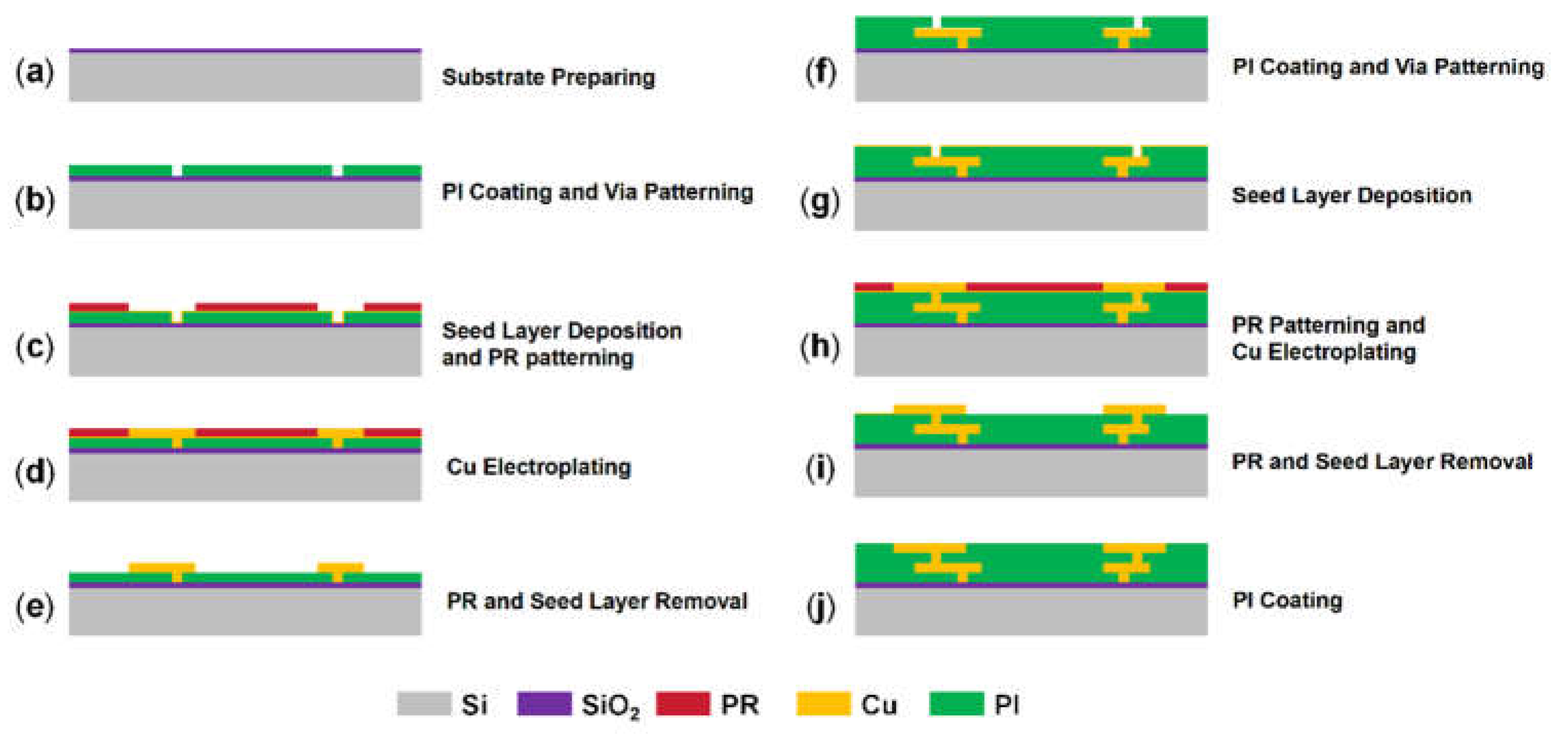
Figure 2.
Top view of the 200-mm RDL wafer sample: (a) Die arrangement on the wafer with dummy structures at the edge. (b) Top view of single die-level region with layout structure.
Figure 2.
Top view of the 200-mm RDL wafer sample: (a) Die arrangement on the wafer with dummy structures at the edge. (b) Top view of single die-level region with layout structure.
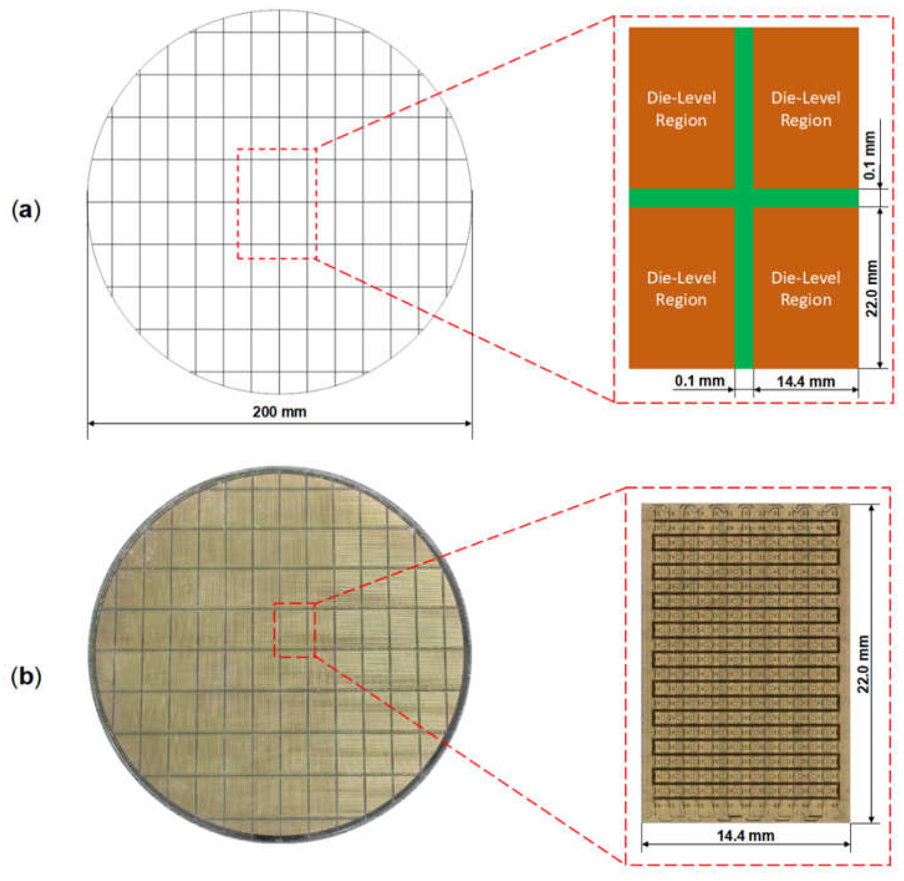
Figure 3.
Two-level partition equivalent processing method for block-level model. (a) Block-level unit with 400× 400 pixels. (b) First partition equivalent processing method. (c) Second partition equivalent processing method.
Figure 3.
Two-level partition equivalent processing method for block-level model. (a) Block-level unit with 400× 400 pixels. (b) First partition equivalent processing method. (c) Second partition equivalent processing method.
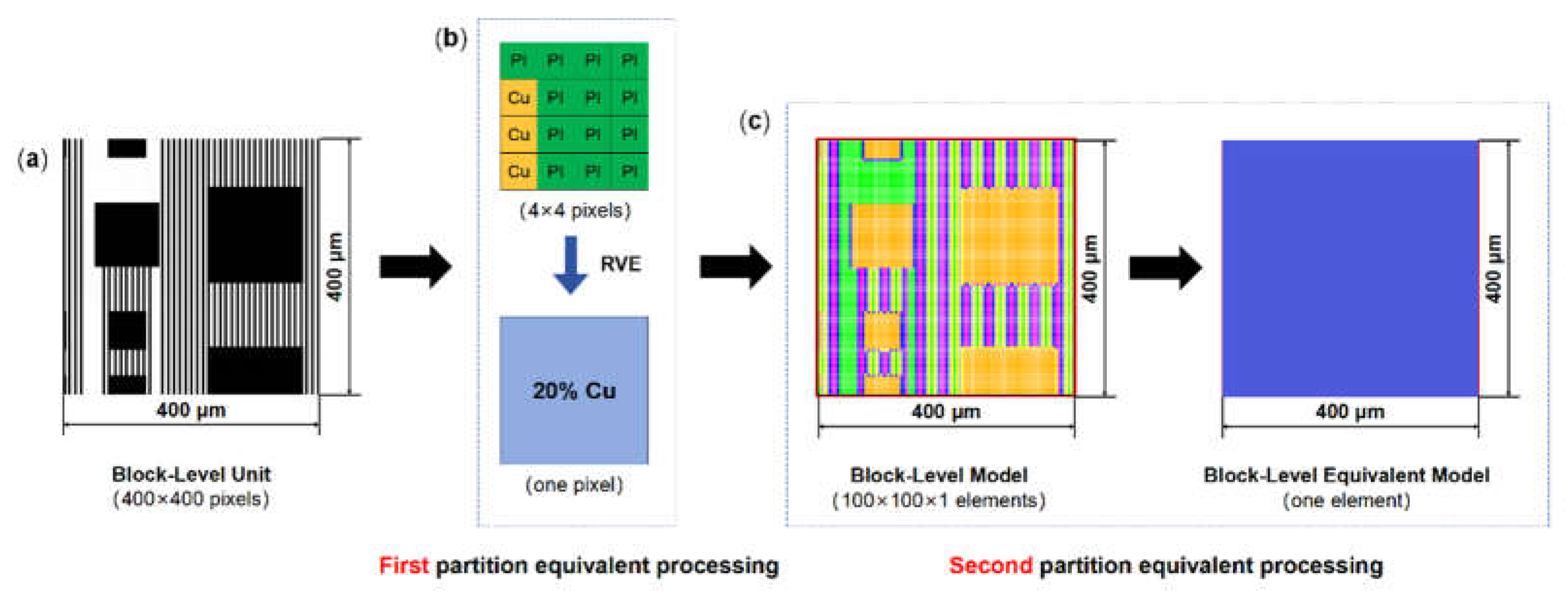
Figure 4.
RDL block equivalent material properties calculation method. With different boundary conditions, the orthotropic material property of RDL Block calculated in ANSYS APDL includes: (a) Young’s modulus in X direction; (b) Young’s modulus in Y direction; (c) Young’s modulus in Z direction; (d) Shear modulus in X-Y plane; (e) Shear modulus in X-Z plane; (f) Shear modulus in Y-Z plane; (g) Thermal conductivity in X direction; (h) Thermal conductivity in Y direction; (i) Thermal conductivity in Z direction; (j) Coefficient of thermal expansion in X/Y/Z directions.
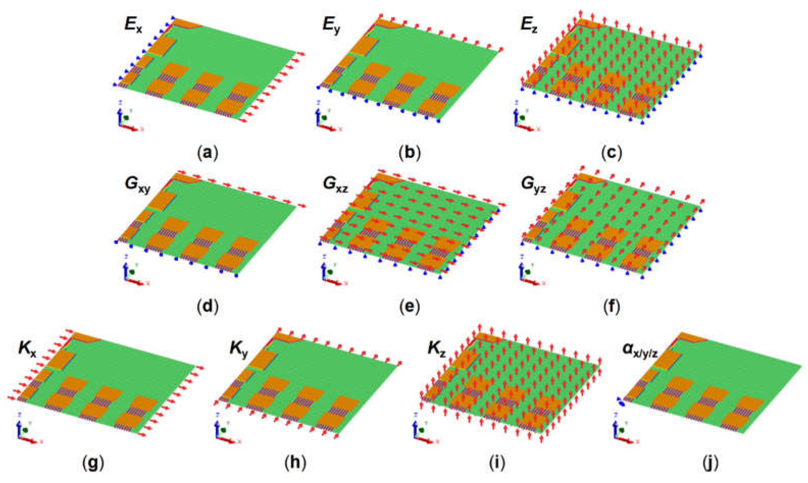
Figure 5.
The method of forming Equivalent Die-Level Model.
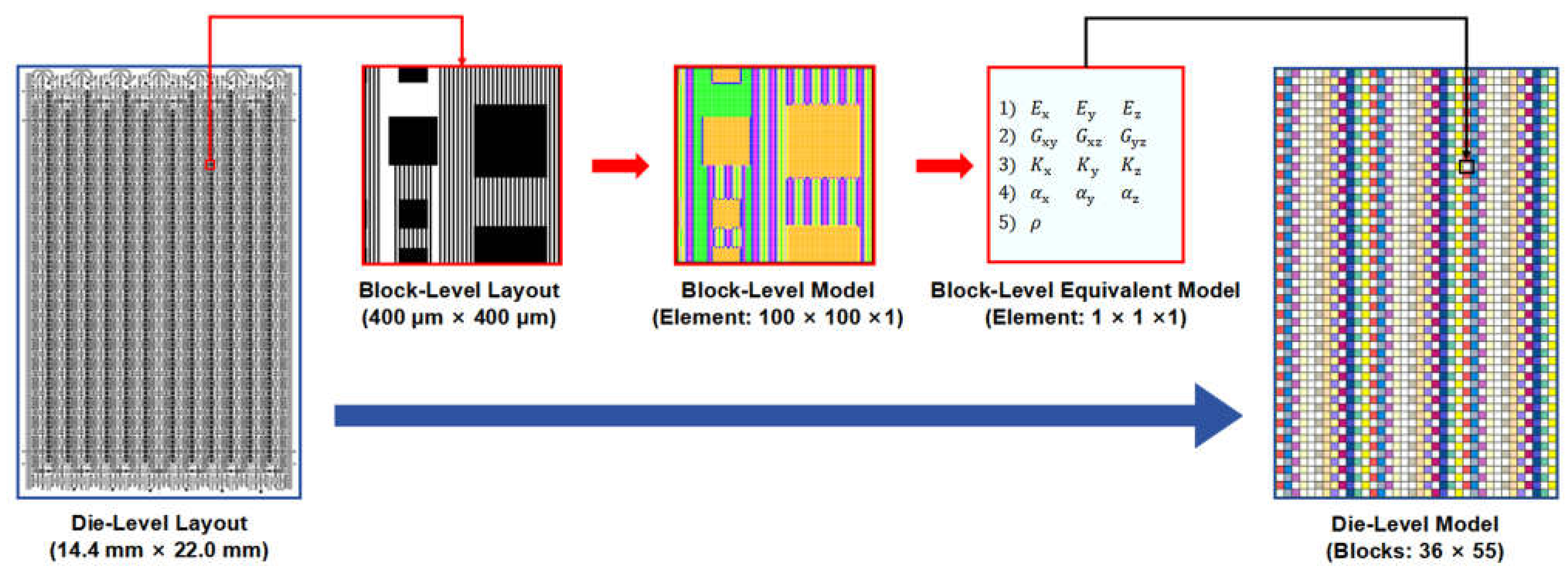
Figure 6.
The details of the equivalent die-level model. (a) Layer layouts of the M1, M2, PI1 and PI2 layers in the die-level region; (b) Layer distribution and thicknesses in the die-level model; (c) Die-level model in Abaqus.
Figure 6.
The details of the equivalent die-level model. (a) Layer layouts of the M1, M2, PI1 and PI2 layers in the die-level region; (b) Layer distribution and thicknesses in the die-level model; (c) Die-level model in Abaqus.
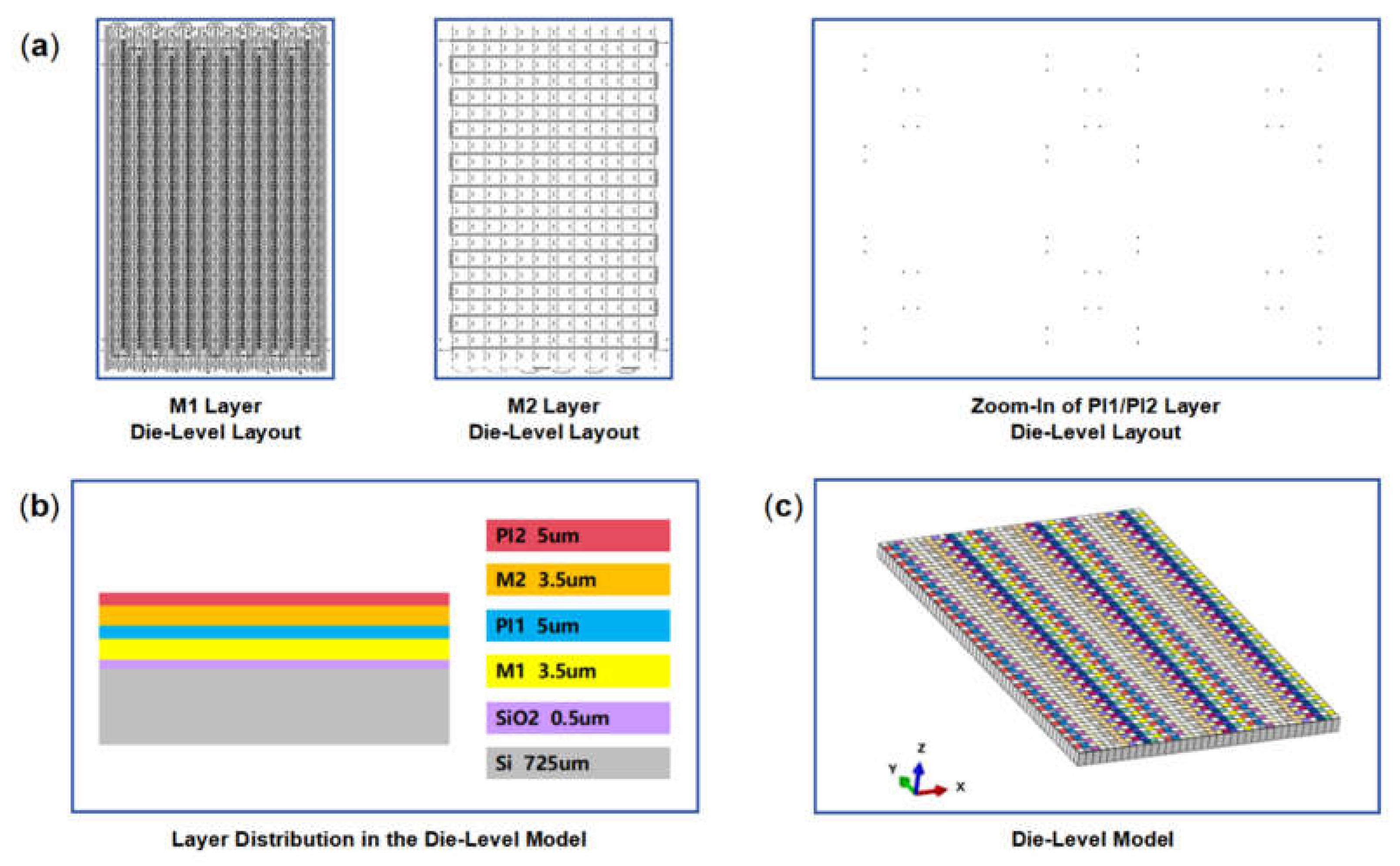
Figure 7.
Equivalent FEM model of the 200-mm RDL Wafer: (a) Wafer-level equivalent model; (b) Side view of the wafer-level equivalent model.
Figure 7.
Equivalent FEM model of the 200-mm RDL Wafer: (a) Wafer-level equivalent model; (b) Side view of the wafer-level equivalent model.

Figure 8.
Thermal warpage test results of the 8-inch PI wafer at different temperature points.
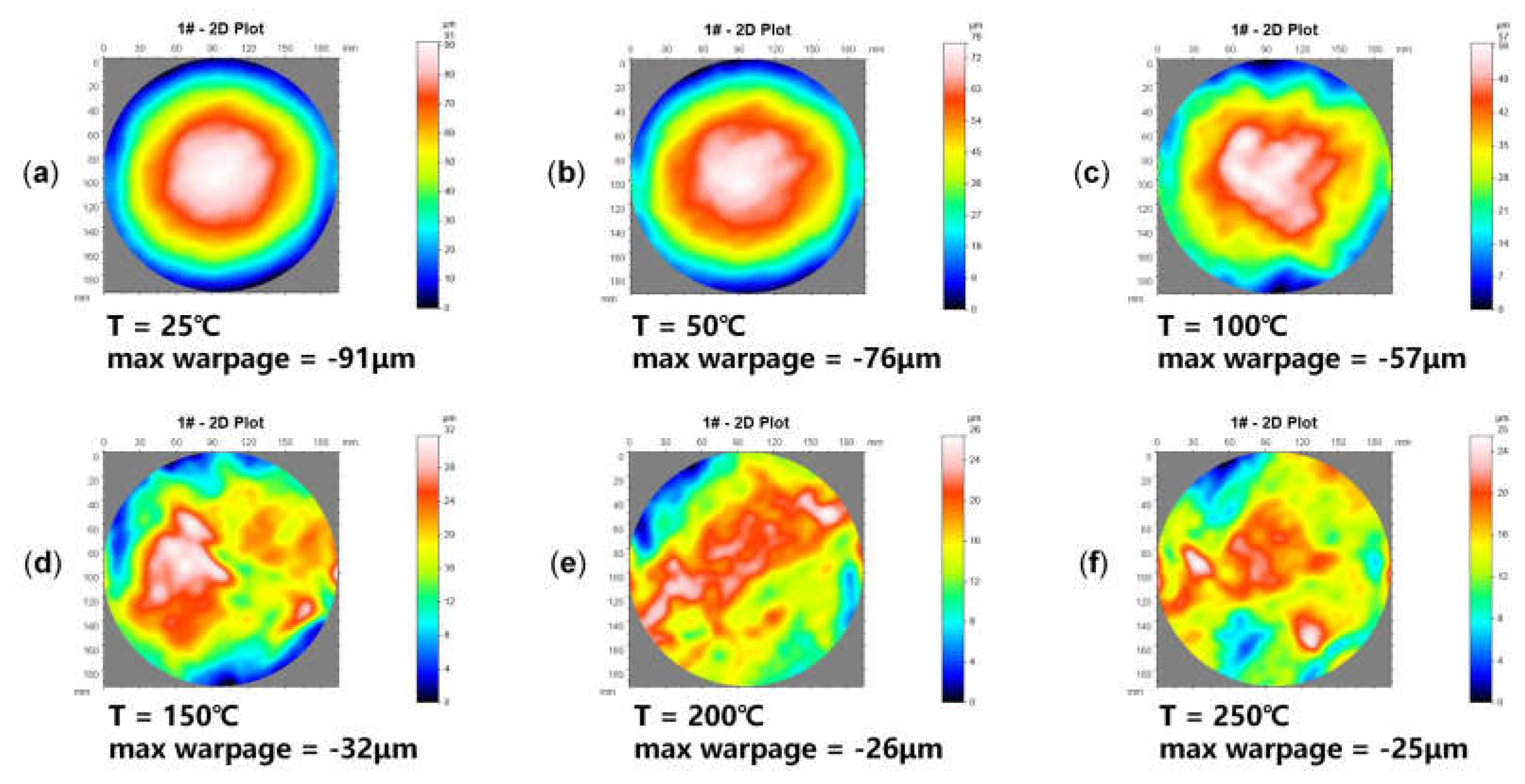
Figure 9.
Thermal warpage simulation results of the 8-inch PI wafer at different temperature points.
Figure 9.
Thermal warpage simulation results of the 8-inch PI wafer at different temperature points.
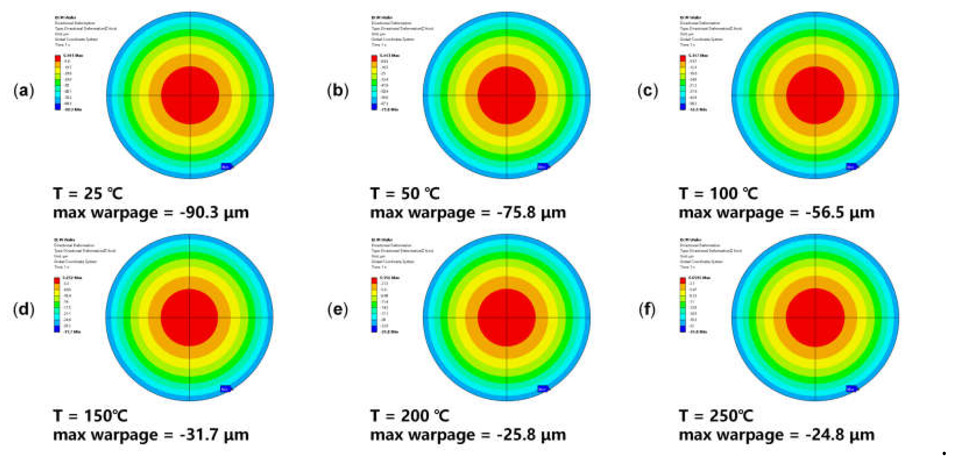
Figure 10.
Measurement and simulation results of 8-inch RDL wafer warpage at typical temperature points.
Figure 10.
Measurement and simulation results of 8-inch RDL wafer warpage at typical temperature points.

Figure 11.
Von-mises stress distribution of the RDL layer at 200℃. (a) Metal 1 layer; (b) Metal 2 layer.
Figure 11.
Von-mises stress distribution of the RDL layer at 200℃. (a) Metal 1 layer; (b) Metal 2 layer.
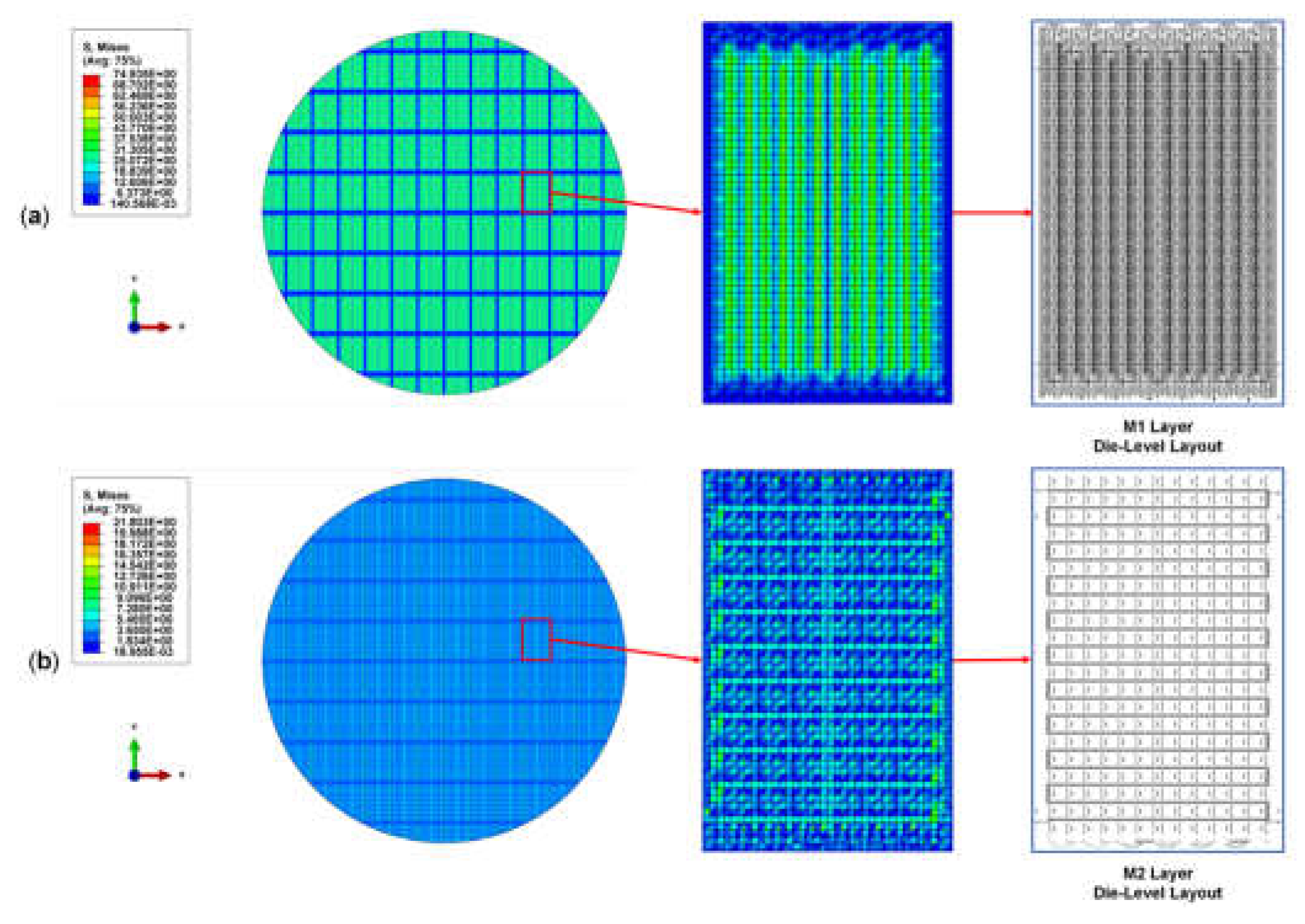
Figure 12.
Prediction results of wafer warpage with different RDL layer counts. (a) Two-layer RDL; (b) Four-layer RDL; (c) Six-layer RDL.
Figure 12.
Prediction results of wafer warpage with different RDL layer counts. (a) Two-layer RDL; (b) Four-layer RDL; (c) Six-layer RDL.
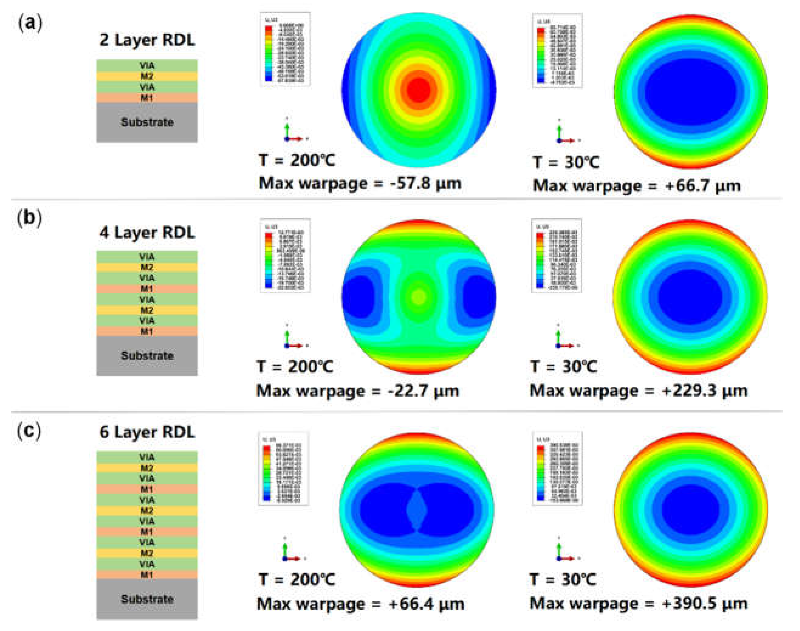
Figure 13.
Process steps of the RDL wafer.

Figure 14.
Prediction results of wafer warpage in different subsequent process steps: (a) Before backgrinding; (b) After backgrinding; (c) After CMP; (d) Adding two-layer back RDL.
Figure 14.
Prediction results of wafer warpage in different subsequent process steps: (a) Before backgrinding; (b) After backgrinding; (c) After CMP; (d) Adding two-layer back RDL.
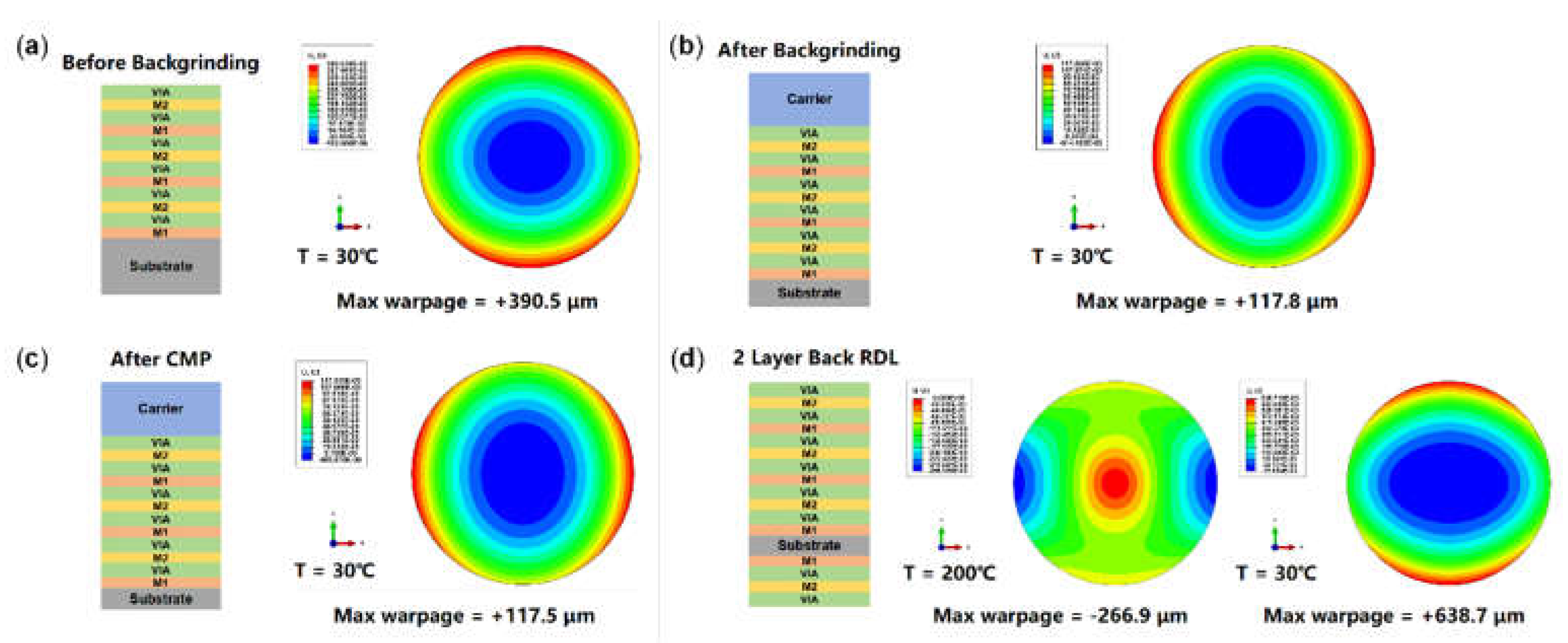
Figure 15.
Prediction results of wafer warpage with different silicon substrate thickness.
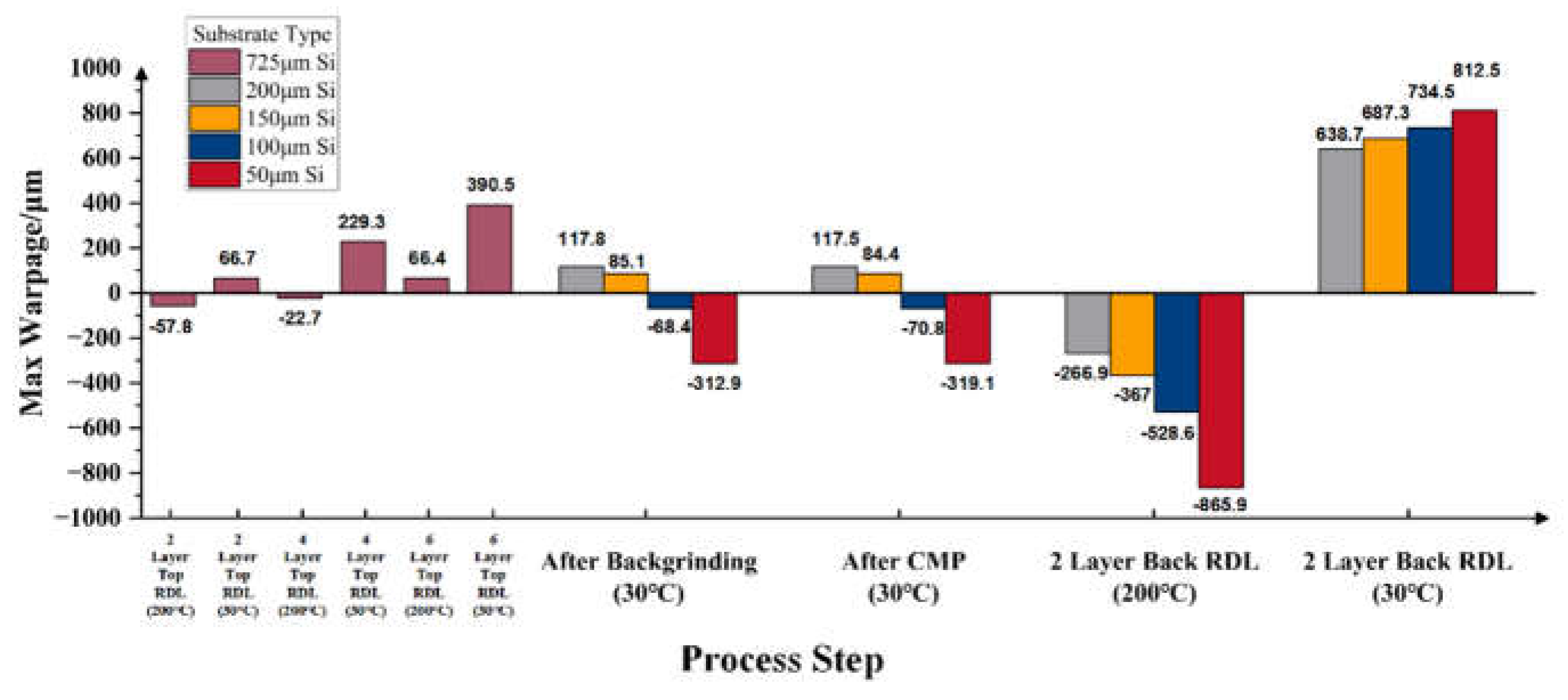
Figure 16.
Warpage prediction contour plots for wafers with different substrate materials after backgrinding, CMP, and the addition of two back RDL layers. (a) Silicon substrate with a thickness of 50 µm. (b) Equivalent TSV substrate with a thickness of 50 µm. (c) Equivalent TGV substrate with a thickness of 50 µm.

Figure 17.
Prediction results of wafer warpage with different equivalent TSV substrate thickness.
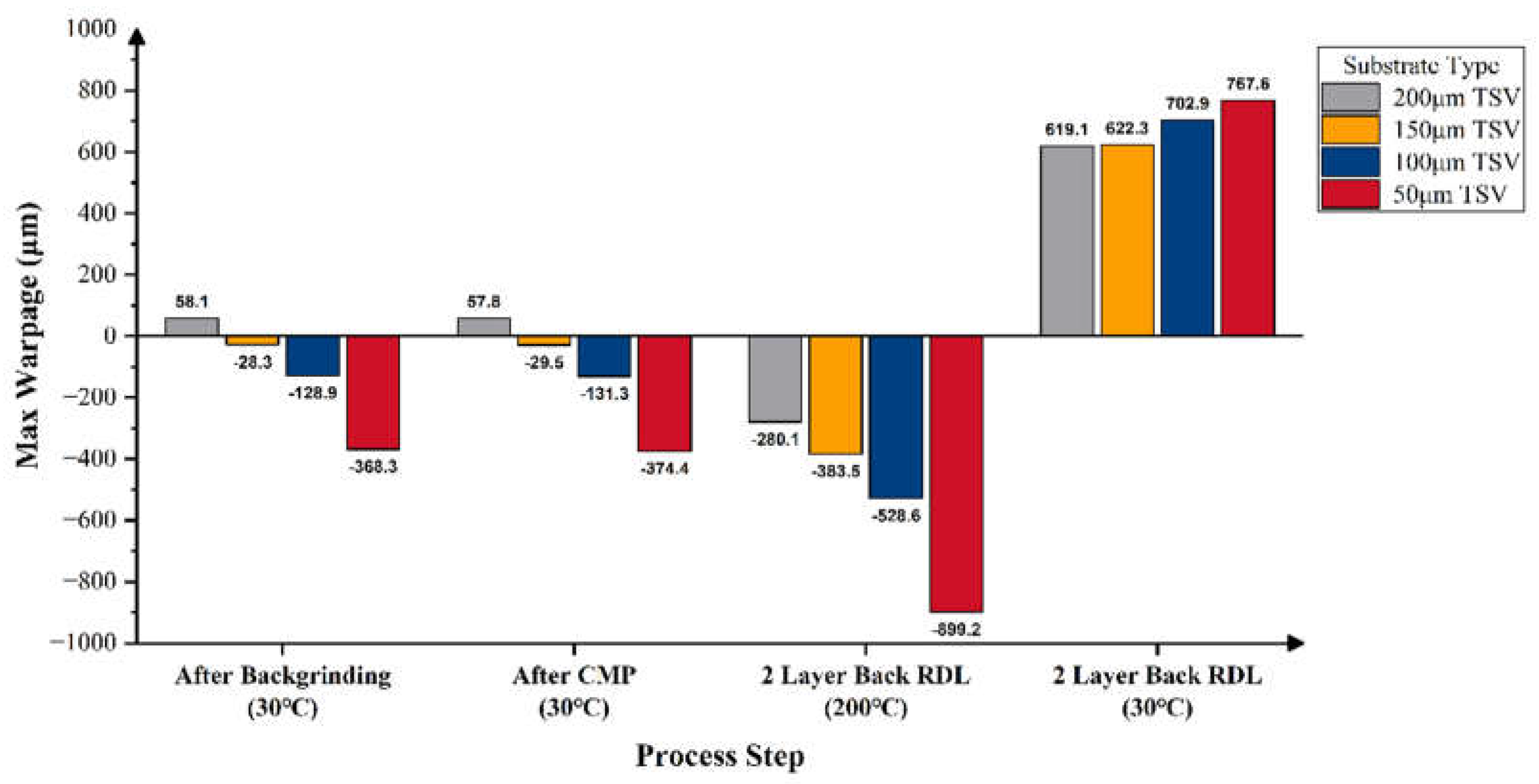
Figure 18.
Prediction results of wafer warpage with different equivalent TGV substrate thickness.
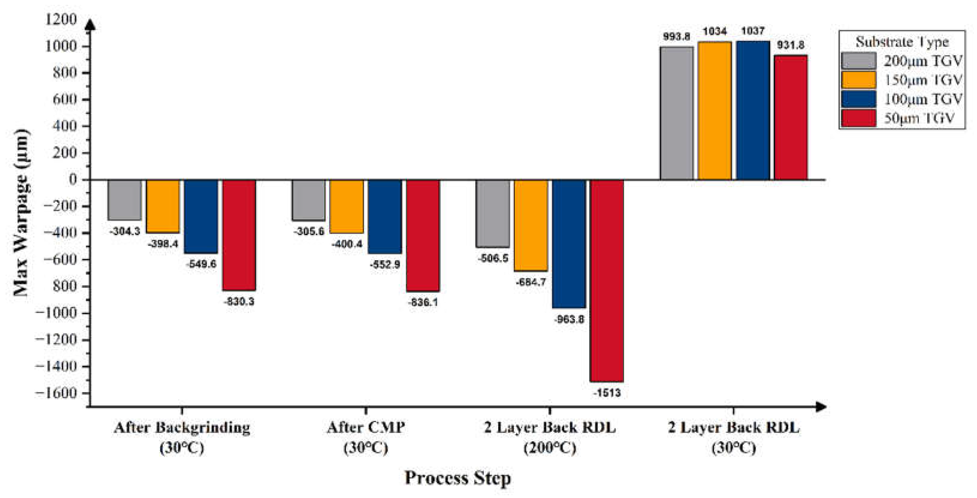
Figure 19.
Establishment of neural network model for predicting warpage. (a) Wafer-level model with four layers RDL and 725-μm-thick glass substrate. (b) Block-Level RDL layouts for different copper proportion. (c) FCNN model for prediction of wafer maximum warpage.
Figure 19.
Establishment of neural network model for predicting warpage. (a) Wafer-level model with four layers RDL and 725-μm-thick glass substrate. (b) Block-Level RDL layouts for different copper proportion. (c) FCNN model for prediction of wafer maximum warpage.
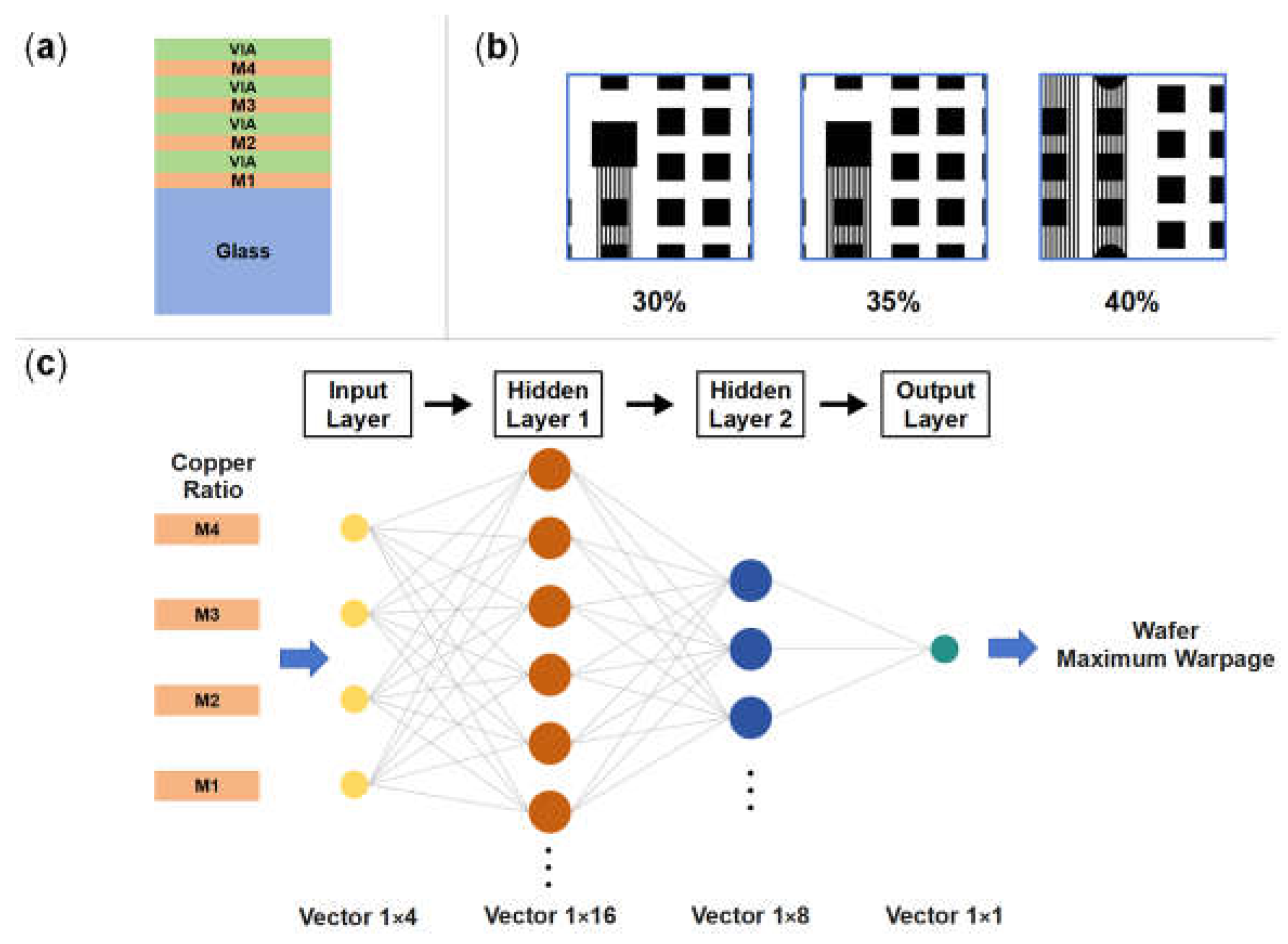
Figure 20.
Predicted warpage results for different RDL copper ratio combination using ANN model.
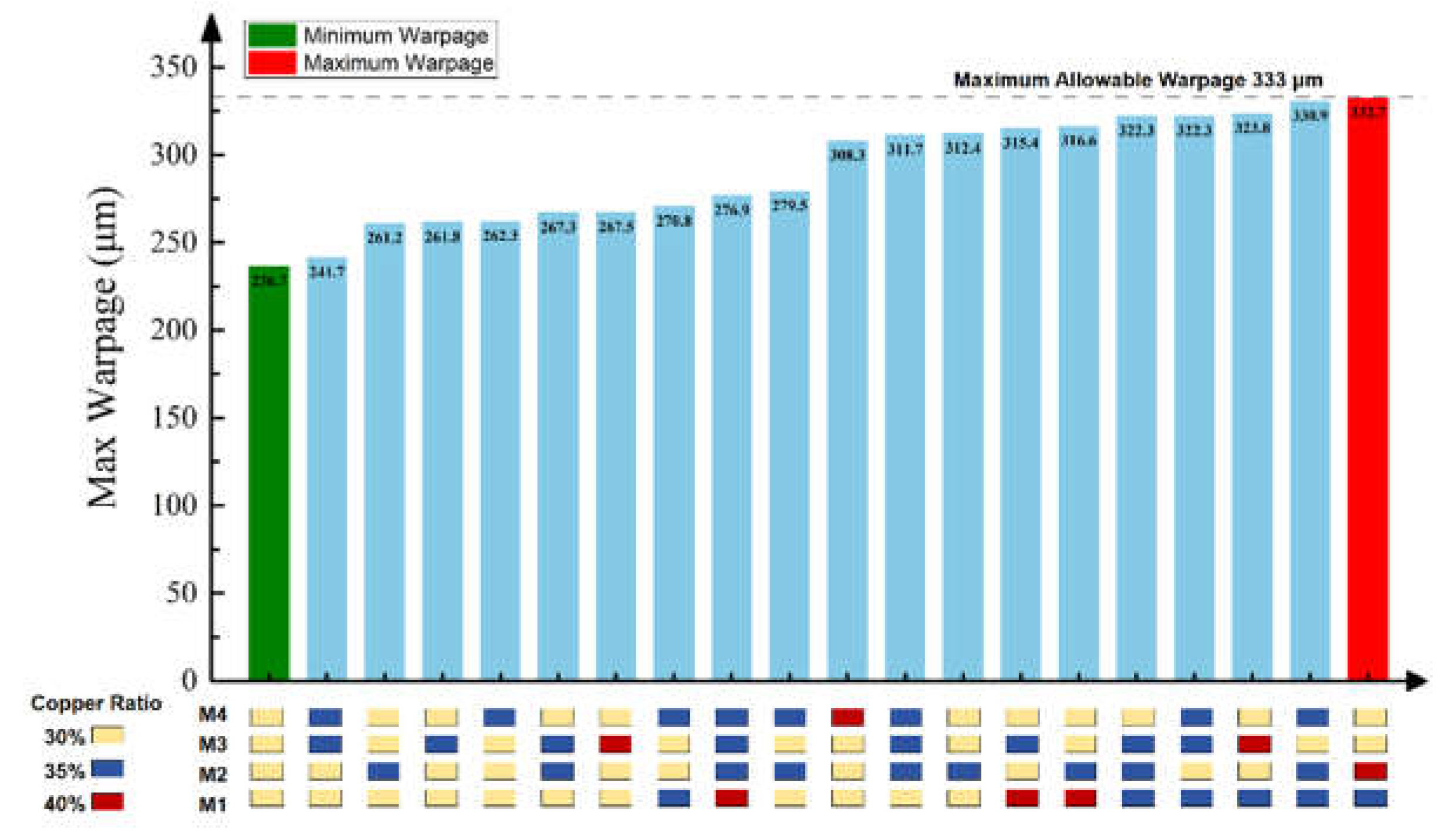

Table 1.
Material properties for simulation analysis of RDL wafer model.
| Materials | Young’s modulus (GPa) |
Poisson’s ratio |
Thermal expansion coefficient (ppm/°C) |
Thermal conductivity (W/m·K) |
Density (kg/m3) |
|---|---|---|---|---|---|
| Si [25] | 131 | 0.28 | 2.6 | 145.87 | 2.329 |
| SiO2 [18] | 73 | 0.17 | 0.55 | 1.1 | 2.300 |
| Cu [26] | 130 | 0.34 | 16.4 | 401 | 8.960 |
| PI | 2.5 | 0.35 | 54 (25℃) 50 (50℃) 47 (100℃) 35 (150℃) 44.5 (200℃) 122 (250℃) |
0.12 | 1.420 |
| Glass | 64 | 0.20 | 3.25 | 1.2 | 2.230 |
Table 2.
Material properties of equivalent TSV substrate with different thickness for simulation analysis.
Table 2.
Material properties of equivalent TSV substrate with different thickness for simulation analysis.
| Materials | Young’s modulus (GPa) |
Poisson’s ratio |
Shear modulus (GPa) |
CTE (ppm/°C) |
Thermal conductivity (W/m·K) |
Density (kg/m3) |
|---|---|---|---|---|---|---|
| Equivalent TSV (h = 50 μm) |
Ex = 130.997868 | νxy = 0.280822 | Gxy = 51.138030 | αx = 2.789632 | Kx = 147.549900 | 2.410 |
| Ey = 130.997868 | νxz = 0.281142 | Gxz = 51.138315 | αy = 2.789632 | Ky = 147.549900 | ||
| Ez = 130.994392 | νyz = 0.281146 | Gyz = 51.138314 | αz = 2.873377 | Kz = 149.000899 | ||
| Equivalent TSV (h = 100 μm) |
Ex = 130.998558 | νxy = 0.280829 | Gxy = 51.138030 | αx = 2.791227 | Kx = 147.549900 | 2.410 |
| Ey = 130.998558 | νxz = 0.280973 | Gxz = 51.138315 | αy = 2.791227 | Ky = 147.549900 | ||
| Ez = 130.994393 | νyz = 0.280975 | Gyz = 51.138315 | αz = 2.828727 | Kz = 149.000899 | ||
| Equivalent TSV (h = 150 μm) |
Ex = 130.998788 | νxy = 0.280831 | Gxy = 51.138030 | αx = 2.791696 | Kx = 147.549899 | 2.410 |
| Ey = 130.998788 | νxz = 0.280931 | Gxz = 51.138315 | αy = 2.791696 | Ky = 147.549899 | ||
| Ez = 130.994393 | νyz = 0.280930 | Gyz = 51.138315 | αz = 2.817442 | Kz = 149.000899 | ||
| Equivalent TSV (h = 200 μm) |
Ex = 130.998903 | νxy = 0.280832 | Gxy = 51.138030 | αx = 2.791925 | Kx = 147.549899 | 2.410 |
| Ey = 130.998903 | νxz = 0.280899 | Gxz = 51.138315 | αy = 2.791925 | Ky = 147.549899 | ||
| Ez = 130.994392 | νyz = 0.280898 | Gyz = 51.138315 | αz = 2.809058 | Kz = 149.000899 |
Table 3.
Material properties of equivalent TGV substrate with different thickness for simulation analysis.
Table 3.
Material properties of equivalent TGV substrate with different thickness for simulation analysis.
| Materials | Young’s modulus (GPa) |
Poisson’s ratio |
Shear modulus (GPa) |
CTE (ppm/°C) |
Thermal conductivity (W/m·K) |
Density (kg/m3) |
|---|---|---|---|---|---|---|
| Equivalent TGV (h = 50 μm) |
Ex = 64.494801 | νxy = 0.201541 | Gxy = 26.838356 | αx = 3.467406 | Kx = 1.229639 | 2.312 |
| Ey = 64.494801 | νxz = 0.201408 | Gxz = 26.857501 | αy = 3.467406 | Ky = 1.229639 | ||
| Ez = 64.831363 | νyz = 0.201373 | Gyz = 26.857501 | αz = 3.703234 | Kz = 6.106258 | ||
| Equivalent TGV (h = 100 μm) |
Ex = 64.494989 | νxy = 0.201543 | Gxy = 26.838356 | αx = 3.468674 | Kx = 1.229639 | 2.312 |
| Ey = 64.494989 | νxz = 0.201344 | Gxz = 26.857501 | αy = 3.468674 | Ky = 1.229639 | ||
| Ez = 64.831363 | νyz = 0.201327 | Gyz = 26.857502 | αz = 3.659611 | Kz = 6.106258 | ||
| Equivalent TGV (h = 150 μm) |
Ex = 64.495051 | νxy = 0.201544 | Gxy = 26.838356 | αx = 3.469015 | Kx = 1.229639 | 2.312 |
| Ey = 64.495051 | νxz = 0.201319 | Gxz = 26.857501 | αy = 3.469015 | Ky = 1.229639 | ||
| Ez = 64.831363 | νyz = 0.201328 | Gyz = 26.857502 | αz = 3.650259 | Kz = 6.106258 | ||
| Equivalent TGV (h = 200 μm) |
Ex = 64.495082 | νxy = 0.201544 | Gxy = 26.838356 | αx = 3.469169 | Kx = 1.229639 | 2.312 |
| Ey = 64.495082 | νxz = 0.201308 | Gxz = 26.857501 | αy = 3.469169 | Ky = 1.229639 | ||
| Ez = 64.831363 | νyz = 0.201317 | Gyz = 26.857502 | αz = 3.641562 | Kz = 6.106258 |
Disclaimer/Publisher’s Note: The statements, opinions and data contained in all publications are solely those of the individual author(s) and contributor(s) and not of MDPI and/or the editor(s). MDPI and/or the editor(s) disclaim responsibility for any injury to people or property resulting from any ideas, methods, instructions or products referred to in the content. |
© 2025 by the authors. Licensee MDPI, Basel, Switzerland. This article is an open access article distributed under the terms and conditions of the Creative Commons Attribution (CC BY) license (https://creativecommons.org/licenses/by/4.0/).
Copyright: This open access article is published under a Creative Commons CC BY 4.0 license, which permit the free download, distribution, and reuse, provided that the author and preprint are cited in any reuse.


