
Submitted:
15 April 2025
Posted:
15 April 2025
You are already at the latest version
Abstract
In the present work a-SiC:H thin films were prepared using magnetron sputtering technique for different substrate temperatures from 100℃ to 290℃. Their optical properties were studied using the ellipsometry technique. The experimental results show that the optical band gap of the films varies from 2.00 eV to 2.18 eV for the hydrogenated films, whereas Eg is equal to 1.29 eV when the film does not contain hydrogen atoms and for Ts=100℃. The optoelectronic quality of the films seems to be the optimum when Ts=100℃ or Ts=220℃. Additionally, the refractive index exhibits an inverse relationship with E₉ as a function of Tₛ. Notably, these thin films were deposited 12 years ago, and their optical properties have remained stable since then.
Keywords:
optical properties
; thin films
; amorphous semiconductors
; silicon carbide
1. Introduction
Amorphous silicon carbide (a-SiC:H) thin films have received considerable attention in recent years due to their unique combination of properties, such us high chemical and mechanical stability, excellent electrical properties and high optical transparency [1]. The optical properties of amorphous silicon carbide (a-SiC:H) thin films, in particular, have made them of great interest in various optoelectronic applications, such as photovoltaics, optoelectronics and gas sensing [2,3]. One of the most important optical properties of a-SiC:H thin films is their optical band gap. In general, a-SiC:H thin films have a wide band gap and this makes them transparent to visible light, but absorbent in the ultraviolet region of the electromagnetic spectrum [4].
Chaussende D. et al. [5] have demonstrated that, between RF power, substrate temperature and pressure, the RF power is the main parameter that, at first order controls all the deposition process and film properties. Generally, the sputtering parameters have been found to have a good influence on both the structural and optical properties of a-SiC thin films [6]. When referring to amorphous films, it is speculated that the optical properties are closely related to the films’ chemical structure. This indicated that by adjusting the sputtering conditions, specifically by changing the concentrations of Si and C atoms, the optical properties of the SiC:H films can be controlled [5,7]. Nussupov K. et al. [7] reported the high suitability of magnetron-sputtered silicon carbide films’ optical properties for reducing surface reflection. In particular, they discovered that the most effective antireflection coating is hydrogenated silicon carbide deposited at 150W RF power.
Another key optical property of a-SiC:H thin films is their refractive index, n. This is a measure of how much light bends when it passes through the material and it determines the optical properties of thin films in optical devices, such as anti-reflection coatings, wavelengths and optical filters. Films deposited at higher power have been shown to exhibit the highest refractive index [7]. Similar to the refractive index, extinction coefficient, k, appears to decrease with decreasing rf power. The decrease in the refractive index with decreasing power could be attributed to a violation of stoichiometry or the presence of voids in the film. It is evident that the transmittance also decreases with a decrease in sputtering power [6].
However, the pressure parameter also affects the refractive index. Kumar M. [6] observed a decrease up to a certain limit of sputtering pressure, followed by an increase with further reduction in sputtering pressure.
The increase of sputtering power also affects the thickness of the films, as it results in a significant increase of the kinetic energy and deposition rate. Thus, the size and shape significantly change, which leads to an increase in the thickness of the films [6]. On the other hand, it is worth noting that during the annealing process, film thickness has been observed to decrease [8]. Additionally, an increase of the plasma power leads to a decrease of both the refractive index and the extinction coefficient. These reductions are attributed to the carbon content of the a-SiC:H film [9].
The optical band gap of c-SiC is known to be larger than that of c-Si [10]. Therefore, the larger the number of Si-C bond fraction exists, the wider the optical band gap appears in the a-Si(1-x)Cx:H thin films. Zhang Y. et al. [10] found that with decreasing the deposition power density, the optical band gap of a-Si(1-x)Cx:H thin films increases due to increasing Si-C bond fraction. Thus, the optical band gap of the a-Si(1-x)Cx:H alloys is controlled through the Si-C bond formed by controlling the deposition power. The same result was found by Kefif K. et al. [11], as well as by Yunaz I. et al. [12].
In addition, by controlling the film composition and deposition conditions we can adjust the absorption coefficient, α. The absorption coefficient of a material is a measure of the amount of light absorbed per unit thickness of the material. The absorption of a-SiC:H thin films is dependent on the film composition and deposition conditions and is typically low for visible light [13].
It is important to note that the increase of Si-C bond fraction increases the concentration of dangling bonds in amorphous thin films, deteriorating their optical properties. This is compensated by introducing the suitable quantity of hydrogen that decreases the dangling bonds concentration.
The main point is the retention of optical properties for the future. The present work focuses on this direction where films were produced 12 years ago.
2. Materials and Methods
The a-SiC:H thin films studied in this work were deposited with the technique of magnetron sputtering. The target used was SiC of constant composition (66 wt% Si and 34 wt% C), 99.9% purity and 81 cm2 in area. The rf power was 150 W and the target to substrate distance was 4.5 cm. The sputtering chamber was evacuated below ≈10-8 Torr before the introduction of argon and hydrogen through variable-leak valves. The substrate temperature was varied from 100℃ up to 290℃. The flow rate of argon was 30 sccm in all cases, whereas the hydrogen flow rate was 20 sccm or 0 sccm for the case of the films not containing hydrogen. The substrate used was Corning glass 7059. The substrate and the target were cleaned by pre-sputtering for about 20min before the deposition of the films. The film thickness and the transmittance spectra of the films were measured using FR-Monitor by ThetaMetrisis.
3. Results
The absorption spectra of the a-SiC:H thin films with different substrate temperatures are shown in Figure 1. Obviously, with increasing substrate temperature, the absorption curves decrease with wavelength, presenting typical behavior for amorphous SiC:H [14]. Data from Figure 1 is used for the calculation of the diagram (figure 2), so as to determine the optical band gaps.
In order to calculate the optical band gaps of the a-SiC:H thin films, the curves have been designed. As it is clear, the a-SiC:H thin films obey the relation obtained by Mott and Davis [15]
where α is the absorption coefficient, B is the Tauc constant [16] and Eg is the optical band gap. The optical band gap is obtained by fitting such absorption data to the above expression.
Figure 3 shows the optical band gap of a-SiC:H films as a function of substrate temperature. It is clear that the Eg, from 100℃ to 290℃, varies from 2.00 eV to 2.18 eV, whereas as the hydrogen flow rate increases from 0 sccm to 20 sccm the Eg increases about 0.8 eV for the case of Ts = 100℃.
From the diagrams of Figure 2 were calculated the values of slope B of the relation (1) and presented in Table 1. Take into account that B is a measure of the disorder of amorphous material and more specifically the highest values represent the less disordered material [17]. It is obvious that the optimum quality material is observed at Ts=100℃ and Ts=220℃.
Table 1 shows the slope B of Tauc constant as a function of substrate temperature. It is clear that maximum value of samples B and D reveals that these films present the minimum disorder, which is related to optimum optoelectronic properties.
Finally, the refractive index, n, of the a-SiC:H thin films deposited with different substrate temperatures was calculated [18] from relation (2):
where
and n1 is the refractive index of the substrate, equal to 1.531 for CORNING-7059 glass and the results are presented in Figure 4.
The results show that the refractive index of a-SiC:H thin films varies within the range of 3.142 to 1.887, where the n of a-SiC thin film is 3.917 which is the highest value. These values are in agreement with the experimental results from previous works on a-SiC:H thin films.
It is important to note that all the samples were deposited 12 years ago , and their optical properties were measured. The same properties were measured again 12 years later and the results remain accurately the same, suggesting that the structure of amorphous material, as well as hydrogen atoms in the network of a-SiC:H, is stable [19]. This property is important for many applications and it is necessary to be supported by other measurements in the near future.
4. Discussion
In this work, samples of amorphous silicon carbide deposited in different substrate temperatures from 100℃ to 290℃ have been studied regarding their optical properties.
It has been established [15] that the addition of hydrogen improves the quality (slope B) and increases the optical band gap significantly, as it reduces the density of states, g(E), near the band gap edges. This is attributed to the fact that hydrogen is being added in order to compensate the dangling bonds in the amorphous network of a-SiC and to reduce the defects of the structure.
Figure 2 shows the (ahν)1/2 versus (hν), where it is obvious that these graphs present different point of intersection with the horizontal axis (hν), as well as different slopes. These results are presented in Figure 3 and Table 1. It is clear that the optical band gap does not present a significant change since substrate temperature increases from 100℃ to 290℃, whereas the absence of hydrogen atoms in a-SiC reduces the Eg up to 0.9 eV. The effect of hydrogen atoms to amorphous thin films has been examined in the past [13,19] since the introduction of hydrogen compensates the dangling bonds and structural defects in a-SiC thin films. The behavior of Eg with the Ts presents deviation from ascending trend, which is observed with a-SiC:H rf sputtered thin films [14] for this temperature range, and can be explained by the fact that for this deposition conditions takes place better rearrangement of hydrogen atoms in the a-SiC:H thin films. This is also supported by the results of slope B (see Table 1) where for Ts=100℃ and Ts=220℃ present the maximum values.
In any case the results of slope B with Ts indicate that it is clear that samples B and D have the optimum compensation of dangling bonds, as well as structure defects, and both are suitable for optoelectronic applications.
It can also be noticed that slope B decreases significantly in sample E, where the hydrogen flow rate is maximum. This is attributed to the fact that when adding foreign atoms to a material, there is a limited concentration that must not be overcome. Hence, if more that the accepted number of atoms are added to the amorphous network, the structure deteriorates and the material quality decreases [20].
5. Conclusions
In the present work the optical properties of a-SiC:H thin films were studied. The films were deposited with magnetron sputtering in different substrate temperature, Ts, from 100℃ up to 290℃ and the main conclusions of the work are the follows;
The experimental results show that the optical band gap, Eg, of a-SIC:H thin films varies from 2.0 eV to 2.18 eV which is attributed to changes in hydrogen concentration in the samples or the structural rearrangement with the increase of Ts. For the case that there aren’t hydrogen atoms in these films, Eg is 1.29eV.
The Tauc slope (B) analysis indicates that films deposited at 100°C and 220°C exhibit the optimal material quality.
The dependence of refractive index, n, on Ts is consistent with the results of Eg.
Finally, the optical properties of the a-SiC:H thin films have remained stable over a 12-year period, demonstrating their reliability for optoelectronic and solar cell applications.
Funding
This research received no external funding.
Conflicts of Interest
The authors declare no conflicts of interest.
References
- Ouadfel, A. M.; Keffous, A.; Kheloufi, A.; Cheriet, A.; Yaddaden, C.; Gabouze, N.; Kechouane, M.; Belkacem, Y.; Boukezzata, A.; Kaci, S.; Talbi, L.; Ouadah, Y.; Bozetine, I.; Rezgui, B.; Guerbous, L.; Menari, H.; Mahmoudi, B.; Menous, I. Silicon Carbide Thin Films with Different Processing Growth as an Alternative for Energetic Application. Optical Materials 2017, 65, 117–123. [Google Scholar] [CrossRef]
- Keffous, A.; Bourenane, K.; Kechouane, M.; Gabouze, N.; Kerdja, T. Morphological, Structural and Optical Properties of Thin SiC Layer Growth onto Silicon by Pulsed Laser Deposition. Vacuum 2007, 81(5), 632–635. [Google Scholar] [CrossRef]
- Myong, S. Y.; Kim, S. S.; Lim, K. S. In Situ Ultraviolet Treatment in an Ar Ambient upon p-Type Hydrogenated Amorphous Silicon–Carbide Windows of Hydrogenated Amorphous Silicon Based Solar Cells. Applied Physics Letters 2004, 84(26), 5416–5418. [Google Scholar] [CrossRef]
- Collins, R.; Taylor, P. C.; Kondo, M.; Carius, R.; Biswas, R. Amorphous and Nanocrystalline Silicon Science and Technology; Cambridge University Press, 2005; Vol. 862.
- Chaussende, D.; Tabouret, V.; Crisci, A.; Morais, M.; Coindeau, S.; Berthomé, G.; Kollmuss, M.; Wellmann, P.; Jomard, F.; Pinault-Thaury, M.-A.; Lu, Y.; Shi, X.; Ou, H. Investigation of Amorphous-SiC Thin Film Deposition by RF Magnetron Sputtering for Optical Applications. Materials Science in Semiconductor Processing 2024, 182, 108673. [Google Scholar] [CrossRef]
- Mukesh Kumar, M. K. Studies of Structural and Optical Properties of Sputtered SiC Thin Films. Zas Mat 2024, 65(2), 343–349. [Google Scholar] [CrossRef]
- Nussupov, K.; Beisenkhanov, N.; Bugybay, Z.; Sultanov, A. Study of Optical and Passivation Properties of Hydrogenated Silicon Carbide Thin Films Deposited by Reactive Magnetron Sputtering for C-Si Solar Cell Application. Thin Solid Films 2023, 782, 140006. [Google Scholar] [CrossRef]
- Künle, M.; Kaltenbach, T.; Löper, P.; Hartel, A.; Janz, S.; Eibl, O.; Nickel, K.-G. Si-Rich a-SiC:H Thin Films: Structural and Optical Transformations during Thermal Annealing. Thin Solid Films 2010, 519(1), 151–157. [Google Scholar] [CrossRef]
- Kwon, S.; Park, Y.; Ban, W.; Youn, C.; Lee, S.; Yang, J.; Jung, D.; Choi, T. Effect of Plasma Power on Properties of Hydrogenated Amorphous Silicon Carbide Hardmask Films Deposited by PECVD. Vacuum 2020, 174, 109187. [Google Scholar] [CrossRef]
- Zhang, Y.; Du, P.; Zhang, R.; Han, G.; Weng, W. Structure and Properties of Hydrogenated Amorphous Silicon Carbide Thin Films Deposited by PECVD. Journal of Non-Crystalline Solids 2008, 354 (12–13), 1435–1439. [CrossRef]
- Kefif, K.; Bouizem, Y.; Belfedal, A.; Sib, J. D.; Benlakehal, D.; Chahed, L. Hydrogen Related Crystallization in Silicon Carbide Thin Films. Optik 2018, 154, 459–466. [Google Scholar] [CrossRef]
- Yunaz, I. A.; Hashizume, K.; Miyajima, S.; Yamada, A.; Konagai, M. Fabrication of Amorphous Silicon Carbide Films Using VHF-PECVD for Triple-Junction Thin-Film Solar Cell Applications. Solar Energy Materials and Solar Cells 2009, 93 (6–7), 1056–1061. [CrossRef]
- Magafas, L.; Kalomiros, J.; Bandekas, D.; Tsirigotis, G. Optimization of the Electrical Properties of Al/a-SiC:H Schottky Diodes by Means of Thermal Annealing of a-SiC:H Thin Films. Microelectronics Journal 2006, 37(11), 1352–1357. [Google Scholar] [CrossRef]
- Magafas, L.; Georgoulas, N.; Girginoudi, D.; Thanailakis, A. The Dependence of Electrical and Optical Properties of RF Sputtered Amorphous Silicon–Carbon Alloy Thin Films on Substrate Temperature and Hydrogen Flow Rate. Phys. Stat. Sol. (a) 1991, 126(1), 143–150. [Google Scholar] [CrossRef]
- Tauc, J. Amorphous and Liquid Semiconductors; Springer: New York, NY, 1974. [Google Scholar]
- Mott, N.; Davis, E. Electronic Processes in Non-Crystalline Materials, 2nd ed.; Clarendon Press, 1979.
- Bullot, J.; Schmidt, M. P. Physics of Amorphous Silicon–Carbon Alloys. Physica Status Solidi (b) 1987, 143(2), 345–418. [Google Scholar] [CrossRef]
- Kalomiros, I. Study of Certain Properties of the Series of the Phyllomorphic Semiconductors mZnS:1ln2S3, Aristotle University of Thessaloniki, 1989.
- Magafas, L.; Bandekas, D.; Boglou, A. K.; Anagnostopoloulos, A. N. Electrical Properties of Annealed A-SiC:H Thin Films. Journal of Non-Crystalline Solids 2007, 353 (11–12), 1065–1069. [CrossRef]
- Kasap, S.; Capper, P. Springer Handbook of Electronic and Photonic Materials; Springer: London, 2006.
Figure 1.
Absorbance coefficient versus wavelength.
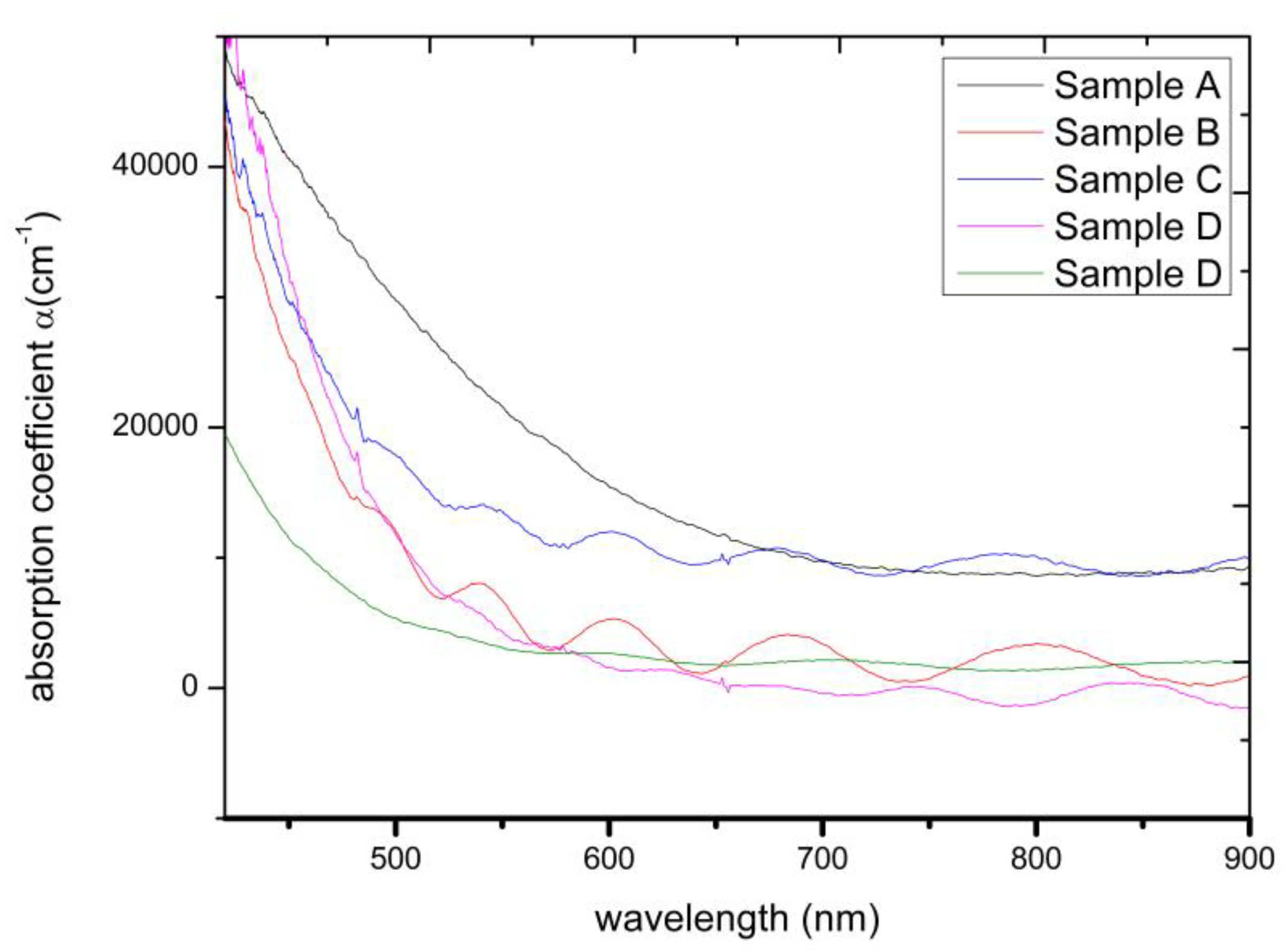
Figure 2.
versus photon energy (hν) and calculation of the optical band gap energies via Mott and Davis method.
Figure 2.
versus photon energy (hν) and calculation of the optical band gap energies via Mott and Davis method.
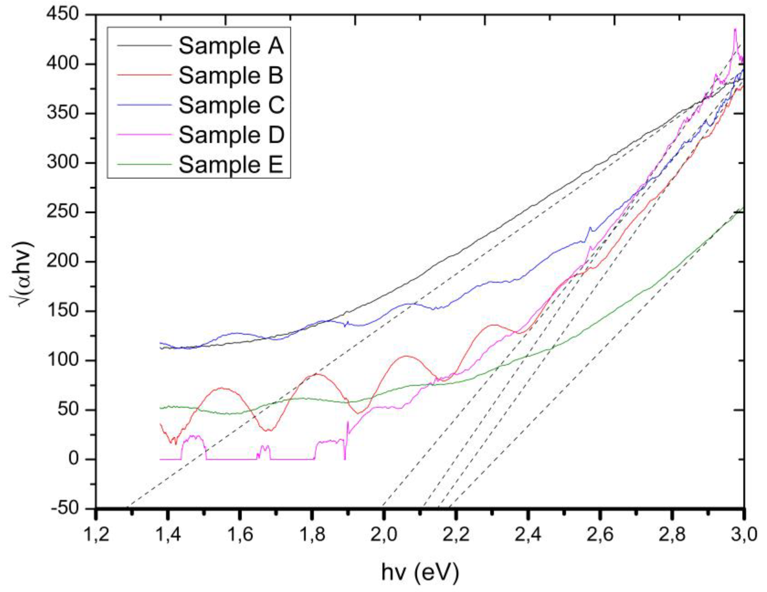
Figure 3.
Optical band gap energy versus substrate temperature.
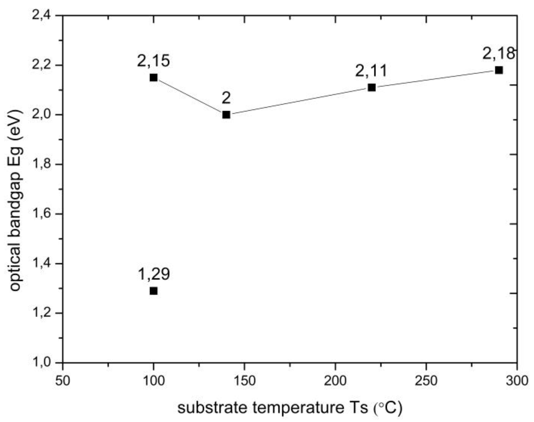
Figure 4.
Refractive index versus substrate temperature.
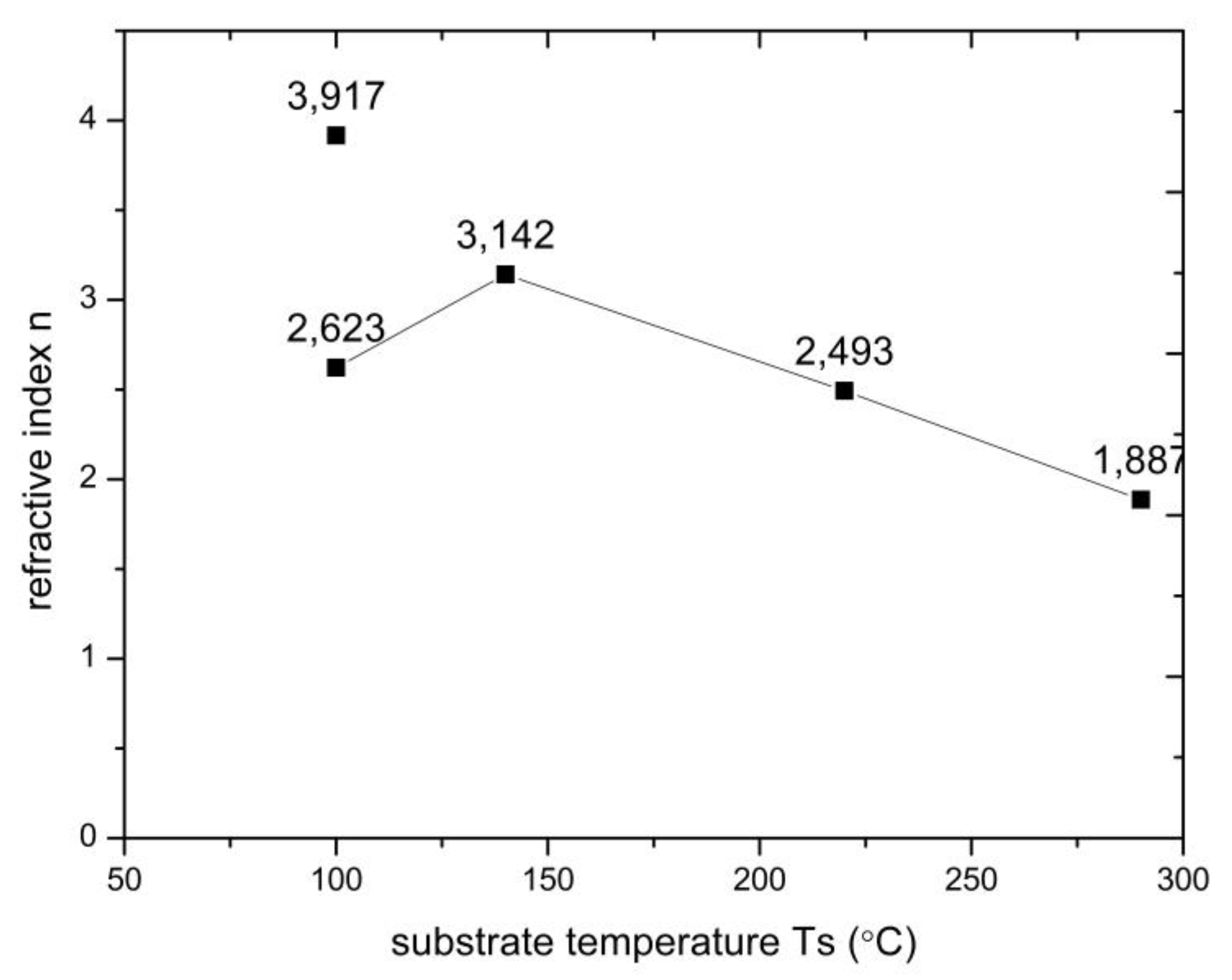

Table 1.
Hydrogen flow rate and Slope B of the obtained a-SiC:H thin films.
| Sample | Substrate Temperature Ts |
Slope B | Hydrogen |
|---|---|---|---|
| A | 224.34 | No | |
| B | 450.93 | Yes | |
| C | 353.63 | Yes | |
| D | 460.32 | Yes | |
| E | 308.38 | Yes |
Disclaimer/Publisher’s Note: The statements, opinions and data contained in all publications are solely those of the individual author(s) and contributor(s) and not of MDPI and/or the editor(s). MDPI and/or the editor(s) disclaim responsibility for any injury to people or property resulting from any ideas, methods, instructions or products referred to in the content. |
© 2025 by the authors. Licensee MDPI, Basel, Switzerland. This article is an open access article distributed under the terms and conditions of the Creative Commons Attribution (CC BY) license (http://creativecommons.org/licenses/by/4.0/).
Copyright: This open access article is published under a Creative Commons CC BY 4.0 license, which permit the free download, distribution, and reuse, provided that the author and preprint are cited in any reuse.


