
Submitted:
18 April 2025
Posted:
21 April 2025
You are already at the latest version
Abstract
Glide-Symmetric Double Corrugated Parallel Plate Waveguides (GS-DCPPWs) has essential technical properties such as electromagnetic bandgap, lower dispersion, and controlling equivalent refractive index. For this reason, fast and simple analysis and design of GS-DCPPW structures have great importance to improve related microwave systems. This paper introduces a novel design methodology, based on the Auxiliary Functions of Generalized Scattering Matrix (AFGSM), for the dimensional synthesis of GS-DCPPWs. We test the applicability of the AFGSM method on a variety of numerical examples to determine the passband/stopband regions of single and GS-DCPPWs before applying the design procedure. Certain design specifications are chosen, and unit cell dimensions are constructed in accordance with the proposed design technique. Three design scenarios are considered to assess the success of how well the design criteria can be met with the proposed method. The designed unit cells have been periodically connected in a various finite number to create periodic filters as a test application for adjusting electromagnetic bandgap. The success of the periodic GS-DCPPW filters obtained with the proposed design strategy in meeting the specified design requirements has been tested using full-wave electromagnetic simulators (CST Microwave Studio and HFSS). The results indicate that the combined use of the equivalent transmission line circuit and the root-finding routine provided by the proposed method facilitates rapid, efficient, versatile, and approximate designs for corrugated parallel plate waveguides. Moreover, the design methodology provides the viability of developing a minimal unit cell and a compact periodic filter performance with respect to literature counterparts.
Keywords:
Corrugated parallel plate waveguides
; dimensional synthesis
; glide symmetry
; periodic filter design
1. Introduction
Electromagnetic properties of periodic structures have been the subject of extensive investigation for many years [1,2,3,4,5]. These structures include properties like how waves move forward and backward and how fast and slow they are, as well as the presence and effect of bandgaps [6,7,8,9]. These significantly higher technical properties have established their role in critical applications, which include antennas [10], frequency selective surfaces [11], filters [9,12,13], and metasurfaces [14]. These components are indispensable to various devices utilized in microwave and millimeter wave applications.
In recent years, analysis, design, and investigation of periodic structures with higher symmetries in microwave applications have gained prominence [15,16,17,18,19,20]. Utilization of these symmetries in periodic structures got its start 50-60 years ago [21,22,23,24]. Glide-symmetric periodic structures, applicable to various geometries [16,22,25,26,27,28,29,30,31,32,33], have been extensively studied by researchers due to their outstanding performance in reducing dispersion, controlling bandgaps and bandwidth, and adjusting the equivalent refractive index for particular applications [17,23]. One of the geometries that implement glide symmetry is Corrugated Parallel Plate Waveguides (CPPWs). These structures are frequently employed in the development of broadband microwave devices [10,24,34,35]. When making microwave devices with CPPW periodic structures that have glide-symmetric corrugations, it is important to first figure out the structure’s dispersion diagram. Dispersion diagram provides critical insights into the attenuation and phase connection of the structure [36].
Recent analyses of dispersion diagrams for these structures have been extensively performed through frequency domain and eigenmode solvers of full-wave electromagnetic simulators, as well as their corresponding designs [25,32,37,38]. In frequency domain solvers, network parameters (S-parameters, ABCD parameters) of the unit cell of periodic structure are determined using multimodal excitation, and dispersion diagram of the periodic structure is derived by substituting the obtained parameters into the eigenvalue equation [3,9,39,40]. Despite complex geometry of periodic structure, it is feasible to precisely derive the dispersion diagram by analysing the behaviour of the eigenvalues using these methods. Nevertheless, full-wave simulators result in excessively prolonged calculation durations. Consequently, the introduction of straightforward and efficient computational techniques will considerably decrease the design duration.
An equivalent circuit model has been recently introduced for the analysis of CPPWs featuring glide-symmetric corrugations [32]. This circuit model is a rapid and effective method that calculates the ABCD parameters of the unit cell and produces dispersion results that are comparable to those of full-wave simulators for a broad spectrum of geometrical parameters as mentioned in [32]. By deriving the circuit model of this structure [32] and obtaining the ABCD or Scattering (S) parameters from the circuit model, the dispersion diagram of the model can only be obtained by solving the eigenvalue equations specified in [32] and [3]. Besides, the Auxiliary Functions of Generalized Scattering Matrix (AFGSM) method [3] is an extremely successful alternative technique that identifies passband and stopband regions of periodic structures by analyzing the zero crossings of auxiliary functions. This method strongly explained in [3] do not need to solve eigenvalue equation (EE). Significantly reduction of computation load can be achieved by this way for controlling bandgaps of periodic structures. It has been previously applied in numerous applications, including rectangular waveguides [3,9], photonic crystals [41], and helix slow wave structures [9,42], to determine the passband/stopband regions of periodic structures and unit cell designs. To the best of our knowledge, the AFGSM method has not been applied to analysis, design, and investigation of CPPW structures with glide-symmetric corrugations.
This study proposes a novel design procedure for one-dimensional glide-symmetric double CPPW structures, based on the AFGSM method for the first time in the open literature. Firstly, we perform analyses to test the effectiveness of the AFGSM method in determining the passband/stopband regions in the considered structures. We compare the results of each analysis with the eigenvalue equation. The next stage involves selecting design requirements and obtaining unit cell designs through dimensional synthesis using the proposed method. This method can yield numerous unit cell dimensions that align with the same design requirements. We evaluate the filtering performances of final designs using finite periodic implementations to understand whether optimal unit cell dimensions determined by the AFGSM method meet the design requirements. The full-wave electromagnetic simulators (HFSS and CST Microwave Studio) is used for testing the filtering performances of unit cells designed with the AFGSM method. We compare the performance of filters designed using the proposed design procedure with the reported literature. One of the main contributions is that we provide here a different perspective to gather networks parameters of CPPW structures by using equivalent transmission line model with their scattering matrices. Graphical illustration of EE and AFGSM methods of single and glide symmetric double CPPW structures are compared for analysis and design stages. Other contribution can be explained from analysis and design results that the presented method can be efficiently utilized for observing electromagnetic bandgap of CPPWs. Another important contributions in this study is giving an ability to minimize the glide-symmetric DCPPW unit cell design for compactness via AFGSM method. Additionally, the auxiliary functions provide a fast design advantage in determining the passband/stopband regions in the structures under examination. The following sections give important information about how to easily use single and glide-symmetric double CPPW periodic structures to find the electromagnetic bandgap and bandwidth using the AFGSM method. The sections also discuss the use of these structures to create a periodic filter using the proposed method as an example application.
2. Materials and Methods
2.1. Theory and Design Strategy
Figure 1 demonstrates single and glide-symmetric double CPPW structures.
Full-wave electromagnetic simulators are capable of modeling these structures to derive their dispersion characteristics. On the other hand, the longitudional transmission line model for these geometries is presented using the circuit model described in [32], as shown in Figure 2. The circuit approach developed by Marcuvitz, with detailed information provided in the appendix and in [43], is utilized for the circuit structure pertinent to this problem. This methodology combines the circuit model from Figure 2 with the necessary parameters from the appendix, resulting in terminals for single and double corrugations with a short circuit configuration. The phase constant of single Floquet mode supported by the unit cell of the periodic structure under consideration can be determined using the following equation [32]:
The parameters , p, , and in Equation (1) represent the Floquet phase constant associated with the periodic structure with respect to the x direction, the unit cell’s period, and the matrix elements A and D, which is function of frequency, of the matrix referring to the unit cell, respectively.
This study will investigate the scattering matrix representation of the unit cell in both the input and output reference planes. We will determine the scattering matrix for each structure in the circuit model inside the unit cell, as illustrated in Figure 2. As shown in Figure 1, the next step is to stack the scattering matrices of these structures on top of each other to get the full set of S-parameters for the corrugated waveguides’ periodic structure. Figure 2 demonstrates the representations of subcircuits. The scattering matrices of the block structures can be seen to cascade from the first block (S1) to the last block (S5), ending with the scattering matrix of the whole structure. S matrices of all models given in Figure 2 (a) and (b) are explained in the appendix. The phase constant for the structure’s dominant mode can be found using the eigenvalue equation given below [3] after getting the unit cell’s S-parameters:
The two parameters and in Equation (2) indicate the scattering parameter components of the unit cell. Full-wave simulators can accomplish multimodal excitation for the unit cell. We can utilize the generalized scattering matrix elements from full-wave simulators to determine the passband and stopband regions of the periodic structure within the following equation [3]:
The AFGSM method can be used for finding band edge frequencies in a symmetric unit cell structure in case of multi mode excitation, and it is described in the literature with the equation below [3]:
There are a total of P modes, with M and being the number of propagating and non-propagating modes in the waveguide used in Equation (4). is the generalized scattering matrix element, and n is the input port that corresponds to the dominant propagating waveguide mode. Single mode propagation can occur when using the circuit model of the CPPW structure given in Figure 2. Besides, reduced form of Equation (4) can be written taking into account equivalent transmission line model only for and :
Equation (5) can only be used for dominant mode, not including higher-order mode interaction. Despite some deviations from design objectives can occur in periodic filter design [44], circuit model can be utilized for fast computing dimensions of unit cells. The designer can significantly reduce computational burden by solving Equation (5) using the root-finding routine, as opposed to using the fine frequency sweeps of Equation (2) to derive the dispersion diagram of glide-symmetric double CPPWs. This fast approach reduces the size of the design space and provides a simple and approximate design method. Unit cell analysis is important for analyzing the dispersion diagram of the periodic structure and establishing approximate solutions. In addition, the finite number of unit cells examined gives the designer an important insight into the compatibility of the passband/stopband regions of the periodic structure and its filtering behavior. Based on this information, the applicability of the AFGSM method for unit cell analysis of corrugated PPW structures and dimensional synthesis of such filters will be tested. Firstly, Equation (5) is applied to determine the passband/stopband regions of a single corrugated PPW, and then the dimensional synthesis of the same structure in accordance with the design requirements is performed. A similar process will be applied for the analysis and dimensional design of glide-symmetric CPPWs. In this context, the following design strategy has been established:
- Step 1: Select single/glide-symmetric double CPPW model and start appropriate unit cell configuration.
- Step 2: Constrain the design space so that the dimensional parameters of the unit cell based on the circuit model given in Figure 2 are in the appropriate range.
- Step 3: Modify the dimensions in the limited design space obtained in Step 2, and determine the appropriate unit cell parameters satisfying the given design requirements employing Equation (5).
- Step 4: Connect the designed unit cells back-to-back a finite number of times to meet the design requirements and obtain the filter responses with full-wave simulators.
3. Results and Discussion
3.1. Numerical Examples
We first investigate the applicability of the AFGSM method for determining the passband and stopband regions of corrugated PPW structures. The final phase is dimensional synthesis in accordance with the design objectives. Figure 3 and Figure 4 illustrate the use of the AFGSM method to simulate wide and narrow stopbands for single and glide-symmetric double CPPWs. The figure captions specify all parameter values. The first and second stopbands of the periodic structure are obtained by applying the eigenvalue equation to the wide stopband example in Figure 3a. These stopbands are located within the ranges of 12.14–19.58 GHz and 29.89–37.26 GHz, respectively. The AFGSM method yields the band edge frequencies of 12.136 GHz, 19.584 GHz, 29.881 GHz, and 37.263 GHz, respectively. The AFGSM method identified the band edges with a maximum difference of 6 MHz, which coincides with the results derived from the eigenvalue equation. Figure 3b presents a narrowband example, indicating the first and second stopband edges at nearly 16.33 GHz, 16.71 GHz, 32.29 GHz, and 33.43 GHz for AFGSM and EE. We achieved band edges near the eigenvalue equation in the narrow stopband scenario, with a maximum deviation of 7 MHz.
Figure 4a,b demonstrate that the zero crossings of the and functions in the AFGSM method consistently align closely with the band edge frequencies in the dispersion diagrams derived from the eigenvalue equation solutions. Floquet mode transitions are observed in certain regions of the dispersion diagrams without stopbands in Figure 4a,b, with transitions occurring at 4.52 GHz and 13.49 GHz, respectively, and 16.57 GHz in Figure 4b. In these regions, the zero crossings of the and functions occur at identical frequencies. Table 1 presents the band edge frequency results associated with Figure 4a,b.
Based on all these analysis results, it is possible to say that Equation (5) provides an alternative way to determine the passband stopband regions of one-dimensional corrugated PPW structures. Furthermore, the AFGSM functions clearly demonstrate the separation of the band edges, even if the stop bandwidth is narrow. The interval division root-finding routine determines the roots of the and functions, eliminating the need for fine frequency sweeps and reducing the computation time by a factor of 6 compared to the eigenvalue equation. In order to apply the dimensional design approach, the following two design objectives are identified.
- (a)
- Ku-band filter design with a suppression level of more than -50 dB in the 15.20-17.78 GHz range for a single CPPWs.
- (b)
- X-band filter design with a suppression level of more than -60 dB in the 8.27-10.91 GHz range for glide-symmetric double CPPWs.
3.2. The Design of Unit Cell and Cascade Connection Analysis Corrugated PPW Structures
The design phase begins with the selection of an appropriate unit cell model. We select the initial parameters = 1 mm, = 1.8 mm, a = 0.8, and b = 2.2 for the air-filled single corrugated PPW model. This selection implements the design procedure as outlined in the initial step. At this point, the design of the unit cell transitions to the determination of the critical parameters of the design geometry. Figure 5 illustrates the relationship between the geometrical parameters of the AFGSM functions and the zero crossings across various frequencies. In the second step, the design procedure maintains the constrained design spaces (with respect to and ) while restricting a and b to specific ranges, as illustrated in Figure 5. The variations given in this figure provide a solution for obtaining the parameters corresponding to the targeted stopband bandwidth for the parameters under investigation. Step 3 investigates the variation of and functions for the dimensions in the limited design space obtained in step 2. Figure 5 illustrates that the and functions for the lines b=2 and a=0.6 possess a stopband that satisfies the design requirements as depicted X and Y point pairs. Determination of the appropriate unit cell parameters is possible through Figure 5. In the final step, Figure 6a shows the dispersion diagram of the designed unit cell, satisfying the suppression level design criterion. We obtained a unit cell design with a stopband of 4.01 GHz bandwidth and a center frequency of 16.51 GHz. To test the band properties, we connected unit cells back to back in varying numbers, as illustrated in Figure 6b. As it is well-known in periodic structures, increasing the number of unit cells leads to a deeper stopband in single CPPWs. In this example, we ensured adequate design requirements by increasing the number of unit cells (N) to 10. Figure 6b shows that the simulation results given by different simulators are quite compatible.
For glide-symmetric double CPPW structures shown in Figure 1b, we set the parameters a=1mm, =0.5mm, ==1mm, and b=12.4mm. This selection implements the design procedure as outlined in the initial step. We limited the a and = parameters to 1-2.5 mm and b to 12.4-13.6 mm at intervals of 0.1 mm by creating multiple design spaces and preserving the glide-symmetry case. This limitation significantly reduces the computational burden in achieving the design requirements. In the design space, the stopband edges of the first stopband region for each parameter are found and recorded using and functions. We obtained a significant data set on a large scale, determining the band edge frequencies determined by the AFGSM functions in the constrained design space. The dataset contains a variety of selectable stopband frequencies and the stopband widths situated at these centers. We have selected a center frequency in this context that can cover the targeted stopband. From this set of data, Equation (5) pulls out the values for different dimensions with a center frequency of 10 GHz, different stop bandwidth values, and a certain frequency deviation (), as shown in Table 2. It is clear from Table 2 that it is possible to obtain different design parameters for the desired bandgap with a certain frequency deviation. At this point, three scenarios, bold and italicized in Table 2, have been selected to meet the design requirements of the dimensional design applicability of Equation (5) for the same and different stop bandwidths.
Figure 7, Figure 8 and Figure 9 illustrates dispersion diagrams and the dominant mode of the frequency characteristics derived from various finite periodic configurations of designed unit cells throughout three selected scenarios. All AFGSM function behaviors and dispersion characteristics of all scenarios given in Figure 7a, Figure 8a and Figure 9a indicate that the roots of the AFGSM functions can efficiently seperate passband stopband regions. The analysis of the filtering characteristics obtained by cascading the unit cells is performed in CST Microwave Studio and HFSS simulation environments. In order to model one-dimensional corrugated PPWs in CST and HFSS, it is necessary to assign appropriate boundary conditions. For this purpose, in CST, electric (Et=0) and magnetic (Ht=0), in HFSS, perfect E and perfect H boundary conditions are assigned to the top, bottom, and side walls of the considered
structures, respectively. It is used the same computer to run the simulations of CST, HFSS and our code of proposed method. Ordinary laptop has Intel (R) Core (TM) i7-6700HQ CPU@2.6GHz with 16 GB RAM. In the examined structures, the firs ten dominant waveguide modes of excitation are satisfied to perform with the waveguide port in CST and with the waveport in HFSS, and the frequency characteristics of the first dominant mode of are investigated. Obtaining the dataset in the given limited design space took 360 hours with CST Eigen Mode Solver, while solving the eigenvalue equation based on the circuit model took 612 seconds. The same dataset was generated in 20 seconds using the AFGSM method. We observe from Figure 7a that Scenario 1’s band edges are 8.648 GHz and 11.344 GHz. In the first scenario, we selected a stop bandwidth of 2.7 GHz and determined the dimensions using the AFGSM functions, with a deviation of 10 MHz. The filtering characteristics of the unit cell designed in Scenario 1 with different numbers of finite periodic arrays are given in Figure 7b. The periodic arrangement of the geometry considered in Scenario 1 significantly increased the passband fluctuation levels as shown in Figure 7b. However, it is evident that the design specifications have not yet reached their target. Selecting unit cell parameters with a broader stopband would prove beneficial in terms of both size and design goals. Figure 8b unequivocally illustrates that a periodic arrangement with N=10 adequately fulfills the design specifications, and the passband ripple levels are considerable. The specified design requirements primarily provide the starting stopband frequency for the suppression level but do not determine the required stop bandwidth in Figure 9b. Additionally, the passband ripple level attains a maximum of -4 dB. Actually, these passband ripple levels given in Figure 7b–Figure 9b can be managed and imporved by employing of broken of glide symmetry as shown in [33]. Another way to eliminate the high ripple level in the passband could be applying tapering technology [45] to unit cell of GS-DCPPWs as a novel study. These techniques are not investigated here due to stopband characteristics of periodic arrangements of GS-DCPPW unit cell are only taking into account for testing purposes. The frequency characteristics of , with a constant unit cell count of for all selected scenarios, are presented in Figure 10.
Table 3 presents the design unit cell parameter values for all scenarios and the overall filter dimensions achieved for N = 10. Currently, there are trade-offs regarding filter performance and dimensions for the scenarios given in Figure 10 and Table 3. Initially, fulfilling the design specifications of Scenario 1 will evidently necessitate an increased number of unit cells. This circumstance will lead to a substantial increase in passband ripple levels. Consequently, Scenario 1 fails to satisfy the design specifications. Scenario 2 satisfies the design specifications with an identical quantity of unit cells, in contrast to the other two scenarios, which utilize varying sizes yet yield the same stopband width. Furthermore, the overall filter length of Scenario 2 is shorter than that of Scenario 3, presenting a compact design possibility. Conversely, while Scenario 3 does not entirely fulfill the design specifications, its ripple levels in the passband surpass those of Scenario 2, thereby providing a design advantage to Scenario 3. Table 3 shows that Scenario 3 provides a compact design that is advantageous in terms of filter height. In glide-symmetrical double CPPWs, the frequency characteristics of , illustrated by the finite periodic combinations in Figure 7b, Figure 8b and Figure 9b, indicate that frequency behaviors of cascaded unit cell begins to approach the center frequency of the stopband depicted in Table 2 as the number of unit cells increases. The situation is important to consider in ascertaining the designer’s design requirements. Utilizing this knowledge, the designer begins the design by selecting a higher stopband center frequency, extracting the unit cell design parameters from the AFGSM functions, and trying to ascertain the design requirements. The AFGSM method finds different solutions that meet the same design criteria. These solutions let you choose the unit cell with the smallest dimension possible, which makes it easier to make small designs.
Table 4 compares the performance of designed periodic bandstop filter with similar performances reported in the open literature. The designed filter exhibits a broader suppression level bandwidth (SLBW) and achieves more compact design according to [3]. Bandstop filter designs based on microstrip technology given in [46,48,49] have notably compact configurations. [46] has similar suppression level with Scenario 2 whereas designed filter demonstrates wider stopband bandwidth. However, [48,49] show higher suppression characteristics and narrow bandwidths with respect to developed filter. One clearly says that despite conventional cavity BPF design given in [47] has small dimensions, the suppression level bandwidth could not be as wide as the designed filter. It can be revealed that although BPF design based on hybrid (microstrip-stripline) technology [47] depicts compact dimensions, developed filter has wider suppression level.
4. Conclusions
This study aimed to investigate the potential of the AFGSM method in analyzing and designing corrugated parallel plate waveguide unit cells. The AFGSM method made it simple to find the passband and stopband regions of single and glide-symmetric double CPPW periodic structures. This method led to the development of a novel design procedure for filter designs with CPPW structures. We demonstrate that we can design glide-symmetric double CPPW filters using the AFGSM method. The design procedure demonstrates the ability to determine the minimum unit cell size. The proposed method and design procedure yield a bandstop filter characteristic that is more compact and has a high degree of suppression bandwidth. Adapting the multimode equivalent circuit model [11] to glide-symmetric periodic structures like GS-DCPPWs and, in this direction, modeling 1D and 2D periodic structures such as frequency selective surfaces [11], holey metasurfaces [25], and corrugated paralel plate waveguide structures [27] for determining band edges using reformulated or novel AFGSM functions and comparing the results with full-wave simulators could be an important future study.
Author Contributions
All authors contributed equally to this work. All authors have read and agreed to the published version of the manuscript.
Funding
This research received no external funding.
Institutional Review Board Statement
Not applicable.
Informed Consent Statement
Not applicable.
Data Availability Statement
The data that support the findings of this study are available from the corresponding author upon reasonable request.
Conflicts of Interest
The authors declare no conflicts of interest.
Abbreviations
The following abbreviations are used in this manuscript:
| MM-GSM | Mode Matching - Generalized Scattering Matrix |
| BSF | Band Stop Filter |
| HFSS | High Frequency Structure Simulator |
| CST | Computer Simulation Technology |
Appendix A. Network Representation Explanation of Expanded Version of Equivalent Circuit of Corrugations
To find the scattering matrices of all structures belonging to the unit cells given in Figure 2, it is necessary to find the scattering matrix of each block element (i=1,2, ...,5). Since blocks S1, S3, and S5 in Figure 2 are conventional transmission lines, the scattering parameters of a lossless transmission line of length l are defined as follows:
By replacing l and with the length and phase constant of the block under consideration, the scattering parameters for blocks S1, S3, and S5 can be found. S2 and S4 circuits play a crucial role in determining the scattering parameters of the unit cells in the corrugated PPW structures under study. To clarify this situation, the open forms of the circuits (S2 and S4) are given in Figure A1a,b, with series stubs reduced in Figure 2.
Figure A1.
Full view of circuit in (a) S2 and (b) S4 blocks given in Figure 2.
Figure A1.
Full view of circuit in (a) S2 and (b) S4 blocks given in Figure 2.
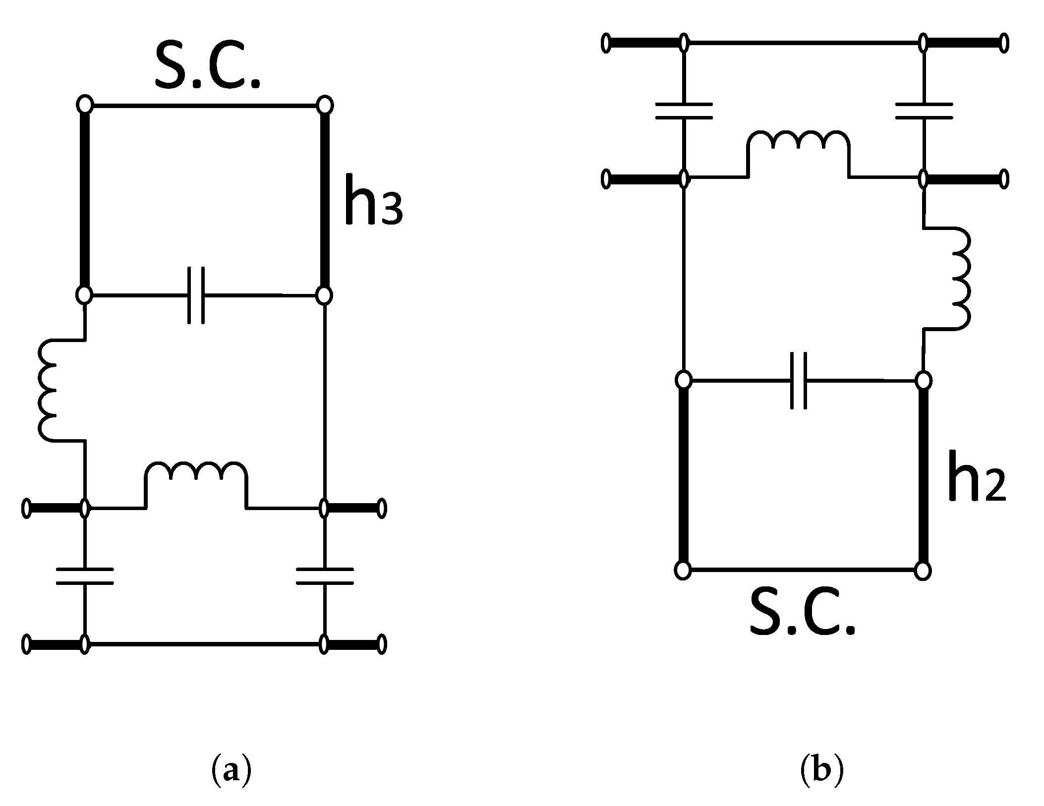
The reactive elements indicated in Figure A1a,b are located at the junctions to account for higher-order mode interactions. The corrugations consist of a series of stubs terminated with a short circuit. Impedance expressions ( and ) for the reduced forms of the circuits mentioned in this work are given. All parametric details of the circuit model’s structure are given in [32] and [43]. The circuits given in Figure A1a,b are symmetrical circuits, and the scattering parameters are defined below:
After the scattering matrices of each (i=1,2,...,5) block circuit are found, the scattering matrices of the blocks are cascaded as [] and [], respectively, by the following equations, and the scattering parameters of the unit cell are obtained.
References
- Pozar, D.M. Microwave engineering: theory and techniques; John wiley & sons, 2021.
- Collin, R.E. Field theory of guided waves; Vol. 5, John Wiley & Sons, 1990.
- Simsek, S.; Topuz, E. Some properties of generalized scattering matrix representations for metallic waveguides with periodic dielectric loading. IEEE transactions on microwave theory and techniques 2007, 11, 2336–2344. [Google Scholar] [CrossRef]
- Ertay, A.O.; Simsek, S. Detection of band edge frequencies in symmetric/asymmetric dielectric loaded helix slow-wave structures. International Journal of Circuit Theory and Applications 2022, 50, 507–524. [Google Scholar] [CrossRef]
- Tahir, G.; Hassan, A.; Ali, S.; Bermak, A. Unit Cell Optimization of Groove Gap Waveguide for High Bandwidth Microwave Applications. Applied Sciences 2024, 14, 10891. [Google Scholar] [CrossRef]
- Şimşek, S.; Topuz, E.; Niver, E. A novel design method for electromagnetic bandgap based waveguide filters with periodic dielectric loading. AEU-International Journal of Electronics and Communications 2012, 66, 228–234. [Google Scholar] [CrossRef]
- Coves, A.; San-Blas, A.A.; Bronchalo, E. Analysis of the dispersion characteristics in periodic Substrate Integrated Waveguides. AEU-International Journal of Electronics and Communications 2021, 139, 153914. [Google Scholar] [CrossRef]
- Mesa, F.; Rodríguez-Berral, R.; Medina, F. On the computation of the dispersion diagram of symmetric one-dimensionally periodic structures. Symmetry 2018, 10, 307. [Google Scholar] [CrossRef]
- Ertay, A.O.; Şimşek, S. A comprehensive auxiliary functions of generalized scattering matrix (AFGSM) method to determine bandgap characteristics of periodic structures. AEU-International Journal of Electronics and Communications 2018, 94, 139–144. [Google Scholar] [CrossRef]
- Liu, Z.; Lu, H.; Liu, J.; Yang, S.; Liu, Y.; Lv, X. Compact fully metallic millimeter-wave waveguide-fed periodic leaky-wave antenna based on corrugated parallel-plate waveguides. IEEE Antennas and Wireless Propagation Letters 2020, 19, 806–810. [Google Scholar] [CrossRef]
- Alex-Amor, A.; Mesa, F.; Palomares-Caballero, Á.; Molero, C.; Padilla, P. Exploring the potential of the multi-modal equivalent circuit approach for stacks of 2-D aperture arrays. IEEE Transactions on Antennas and Propagation 2021, 69, 6453–6467. [Google Scholar] [CrossRef]
- Xu, S.; Wu, J.; Chen, X. Design of Broadband Highly Efficient Power Amplifier Based on Low-Pass Filtering Network With Periodic Structure. International Journal of Circuit Theory and Applications 2024. [Google Scholar] [CrossRef]
- Karamirad, M.; Pouyanfar, N.; Alibakhshikenari, M.; Ghobadi, C.; Nourinia, J.; See, C.H.; Falcone, F. Low-loss and dual-band filter inspired by glide symmetry principle over millimeter-wave spectrum for 5G cellular networks. Iscience 2023, 26. [Google Scholar] [CrossRef]
- Maci, S.; Minatti, G.; Casaletti, M.; Bosiljevac, M. Metasurfing: Addressing waves on impenetrable metasurfaces. IEEE Antennas and Wireless Propagation Letters 2011, 10, 1499–1502. [Google Scholar] [CrossRef]
- Quevedo-Teruel, O.; Valerio, G.; Sipus, Z.; Rajo-Iglesias, E. Periodic structures with higher symmetries: Their applications in electromagnetic devices. IEEE Microwave Magazine 2020, 21, 36–49. [Google Scholar] [CrossRef]
- Palomares-Caballero, Á.; Alex-Amor, A.; Padilla, P.; Valenzuela-Valdés, J.F. Dispersion and filtering properties of rectangular waveguides loaded with holey structures. IEEE Transactions on Microwave Theory and Techniques 2020, 68, 5132–5144. [Google Scholar] [CrossRef]
- Quevedo-Teruel, O.; Chen, Q.; Mesa, F.; Fonseca, N.J.; Valerio, G. On the benefits of glide symmetries for microwave devices. IEEE Journal of Microwaves 2021, 1, 457–469. [Google Scholar] [CrossRef]
- Ghasemifard, F.; Norgren, M.; Quevedo-Teruel, O. Twist and polar glide symmetries: an additional degree of freedom to control the propagation characteristics of periodic structures. Scientific reports 2018, 8, 1–7. [Google Scholar] [CrossRef]
- Dahlberg, O.; Mitchell-Thomas, R.; Quevedo-Teruel, O. Reducing the dispersion of periodic structures with twist and polar glide symmetries. Scientific reports 2017, 7, 10136. [Google Scholar] [CrossRef]
- Arnberg, P.; Barreira Petersson, O.; Zetterstrom, O.; Ghasemifard, F.; Quevedo-Teruel, O. High refractive index electromagnetic devices in printed technology based on glide-symmetric periodic structures. Applied Sciences 2020, 10, 3216. [Google Scholar] [CrossRef]
- Hessel, A.; Chen, M.H.; Li, R.C.; Oliner, A.A. Propagation in periodically loaded waveguides with higher symmetries. Proceedings of the IEEE 1973, 61, 183–195. [Google Scholar] [CrossRef]
- Ebrahimpouri, M.; Quevedo-Teruel, O.; Rajo-Iglesias, E. Design guidelines for gap waveguide technology based on glide-symmetric holey structures. IEEE microwave and wireless components letters 2017, 27, 542–544. [Google Scholar] [CrossRef]
- Tamayo-Dominguez, A.; Fernandez-Gonzalez, J.M.; Quevedo-Teruel, O. One-plane glide-symmetric holey structures for stop-band and refraction index reconfiguration. Symmetry 2019, 11, 495. [Google Scholar] [CrossRef]
- Quevedo-Teruel, O.; Ebrahimpouri, M.; Kehn, M.N.M. Ultrawideband metasurface lenses based on off-shifted opposite layers. IEEE Antennas and Wireless Propagation Letters 2015, 15, 484–487. [Google Scholar] [CrossRef]
- Ghasemifard, F.; Norgren, M.; Quevedo-Teruel, O.; Valerio, G. Analyzing glide-symmetric holey metasurfaces using a generalized Floquet theorem. IEEE Access 2018, 6, 71743–71750. [Google Scholar] [CrossRef]
- Herran, L.F.; Chen, Q.; Mesa, F.; Quevedo-Teruel, O. Electromagnetic Bandgap Based on a Compact Three-Hole Double-Layer Periodic Structure. IEEE Transactions on Antennas and Propagation 2023. [Google Scholar] [CrossRef]
- Ghasemifard, F.; Norgren, M.; Quevedo-Teruel, O. Dispersion analysis of 2-D glide-symmetric corrugated metasurfaces using mode-matching technique. IEEE Microwave and Wireless Components Letters 2017, 28, 1–3. [Google Scholar] [CrossRef]
- Valerio, G.; Ghasemifard, F.; Sipus, Z.; Quevedo-Teruel, O. Glide-symmetric all-metal holey metasurfaces for low-dispersive artificial materials: Modeling and properties. IEEE Transactions on Microwave Theory and Techniques 2018, 66, 3210–3223. [Google Scholar] [CrossRef]
- Fischer, B.; Valerio, G. Dispersion properties of glide-symmetric corrugated metasurface waveguides. International Journal of Microwave and Wireless Technologies 2024, 16, 13–20. [Google Scholar] [CrossRef]
- Memeletzoglou, N.; Sanchez-Cabello, C.; Pizarro-Torres, F.; Rajo-Iglesias, E. Analysis of periodic structures made of pins inside a parallel plate waveguide. Symmetry 2019, 11, 582. [Google Scholar] [CrossRef]
- Chen, Q.; Mesa, F.; Yin, X.; Quevedo-Teruel, O. Accurate characterization and design guidelines of glide-symmetric holey EBG. IEEE Transactions on Microwave Theory and Techniques 2020, 68, 4984–4994. [Google Scholar] [CrossRef]
- Valerio, G.; Sipus, Z.; Grbic, A.; Quevedo-Teruel, O. Accurate equivalent-circuit descriptions of thin glide-symmetric corrugated metasurfaces. IEEE Transactions on Antennas and Propagation 2017, 65, 2695–2700. [Google Scholar] [CrossRef]
- Ertay, A.O. Modeling, Analysis, and Comparison of Rectangular Waveguide Structures Having Glide Symmetrical Step Discontinuity with Periodic Dielectric Loading. Erzincan University Journal of Science and Technology 2024, 17, 826–839. [Google Scholar] [CrossRef]
- Fischer, B.; Valerio, G. Quasi-static homogenization of glide-symmetric holey parallel-plate waveguides with ultra-wideband validity. IEEE Transactions on Antennas and Propagation 2022, 70, 10569–10582. [Google Scholar] [CrossRef]
- Lai, W.Y.; Kehn, M.N.M. Analysis of Rotated Corrugated Parallel Plate Waveguide Using Asymptotic Corrugation Boundary Conditions. In Proceedings of the 2019 IEEE International Symposium on Antennas and Propagation and USNC-URSI Radio Science Meeting. IEEE; 2019; pp. 837–838. [Google Scholar]
- Mesa, F.; Valerio, G.; Rodriguez-Berral, R.; Quevedo-Teruel, O. Simulation-assisted efficient computation of the dispersion diagram of periodic structures: A comprehensive overview with applications to filters, leaky-wave antennas and metasurfaces. IEEE Antennas and Propagation Magazine 2020, 63, 33–45. [Google Scholar] [CrossRef]
- Castillo-Tapia, P.; Mesa, F.; Yakovlev, A.; Valerio, G.; Quevedo-Teruel, O. Study of forward and backward modes in double-sided dielectric-filled corrugated waveguides. Sensors 2021, 21, 6293. [Google Scholar] [CrossRef] [PubMed]
- Castillo-Tapia, P.; Mesa, F.; Quevedo-Teruel, O. Multimodal Transfer Matrix Approach for the Analysis and Fundamental Understanding of Periodic Structures with Higher Symmetries. In Proceedings of the 2022 16th European Conference on Antennas and Propagation (EuCAP). IEEE; 2022; pp. 1–5. [Google Scholar]
- Castillo-Tapia, P. The Multimodal Transfer Matrix Method: And its application to higher-symmetric periodic structures. PhD thesis, KTH Royal Institute of Technology, 2022.
- Lech, R.; Mazur, J. Propagation in rectangular waveguides periodically loaded with cylindrical posts. IEEE microwave and wireless components letters 2004, 14, 177–179. [Google Scholar] [CrossRef]
- Şimşek, S. A fast and accurate design method for broad omnidirectional bandgaps of one dimensional photonic crystals. AEU-International Journal of Electronics and Communications 2014, 68, 865–868. [Google Scholar] [CrossRef]
- Ertay, A.O.; Şimşek, S. Determination of stopband characteristics of asymmetrically loaded helix slow wave structures with Auxiliary Functions of Generalized Scattering Matrix (AFGSM) method. AEU-International Journal of Electronics and Communications 2018, 95, 271–278. [Google Scholar] [CrossRef]
- Marcuvitz, N. Waveguide handbook; P. Peregrinus on behalf of the Institution of Electrical Engineers, 1986.
- Şimşek, S.; Rezaeieh, S.A. A design method for substrate integrated waveguide electromagnetic bandgap (SIW-EBG) filters. AEU-International Journal of Electronics and Communications 2013, 67, 981–983. [Google Scholar] [CrossRef]
- Zhu, H.; Mao, J. Miniaturized tapered EBG structure with wide stopband and flat passband. IEEE Antennas and Wireless Propagation Letters 2012, 11, 314–317. [Google Scholar]
- Ertay, A.O.; Şimşek, S. A compact bandstop filter design for X-band applications. In Proceedings of the 2016 International Symposium on Fundamentals of Electrical Engineering (ISFEE). IEEE; 2016; pp. 1–6. [Google Scholar]
- Hou, F.; Li, L.; Shen, Y.; Sun, C.; Luan, H.; Hu, S. Wideband switchable sharp-rejection filter in compact 3-D heterogeneous integration. IEEE Transactions on Components, Packaging and Manufacturing Technology 2022, 12, 1583–1590. [Google Scholar] [CrossRef]
- Reines, I.; Park, S.J.; Rebeiz, G.M. Compact low-loss tunable X-band bandstop filter with miniature RF-MEMS switches. IEEE Transactions on Microwave Theory and Techniques 2010, 58, 1887–1895. [Google Scholar] [CrossRef]
- Zheng, G.; Papapolymerou, J. Monolithic reconfigurable bandstop filter using RF MEMS switches. International Journal of RF and Microwave Computer-Aided Engineering: Co-sponsored by the Center for Advanced Manufacturing and Packaging of Microwave, Optical, and Digital Electronics (CAMPmode) at the University of Colorado at Boulder 2004, 14, 373–382. [Google Scholar] [CrossRef]
Figure 1.
Unit cell geometries of 1-D Corrugated Paralel Plate Waveguide (a) single CPPW (b) glide-symmetric CPPW. As mentioned in [32], if and , the unit cell has glide-symmetry.
Figure 1.
Unit cell geometries of 1-D Corrugated Paralel Plate Waveguide (a) single CPPW (b) glide-symmetric CPPW. As mentioned in [32], if and , the unit cell has glide-symmetry.
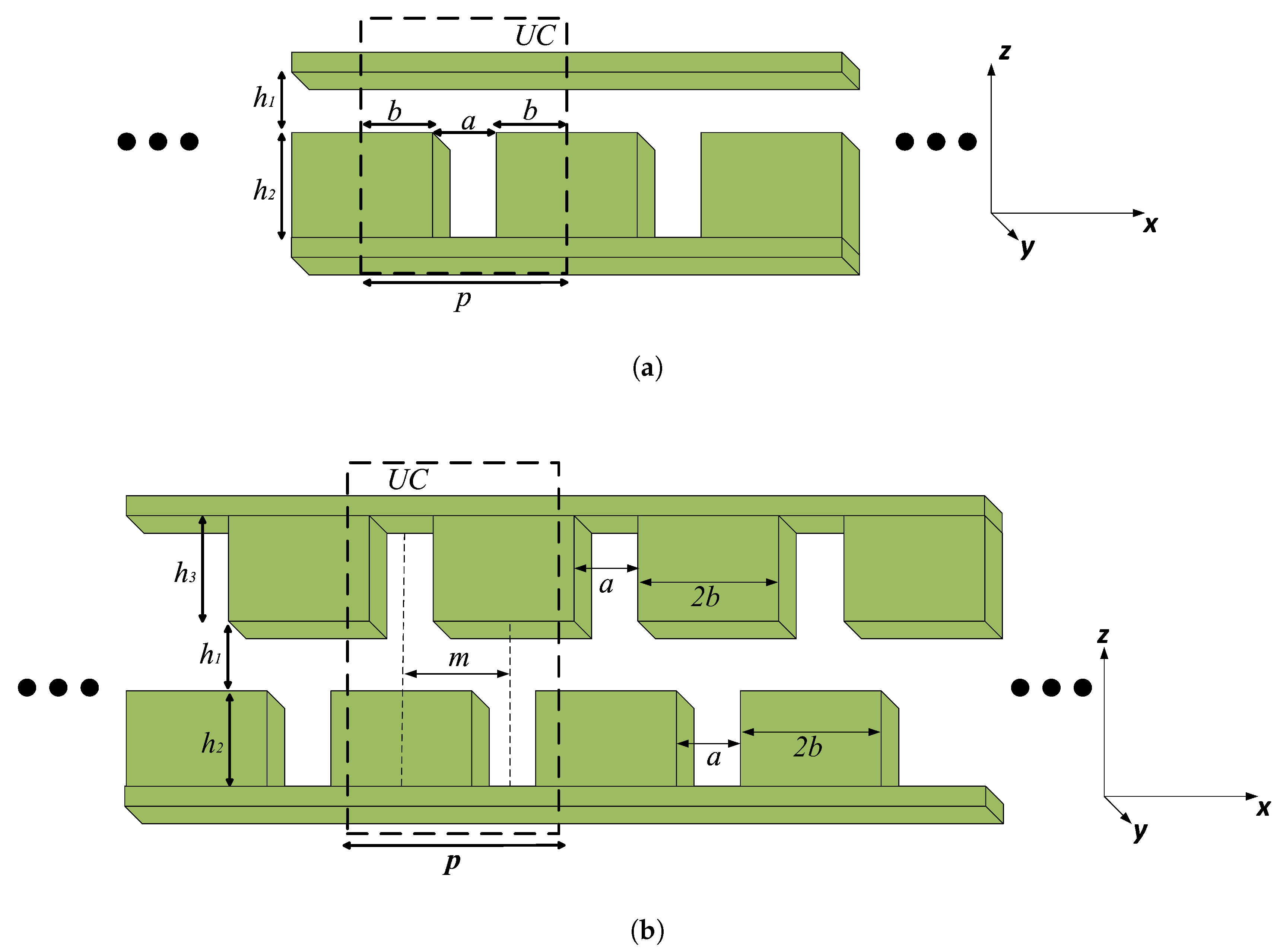
Figure 2.
Equivalent circuit model of (a) single corrugated and (b) glide symmetric double corrugated PPW structures.
Figure 2.
Equivalent circuit model of (a) single corrugated and (b) glide symmetric double corrugated PPW structures.
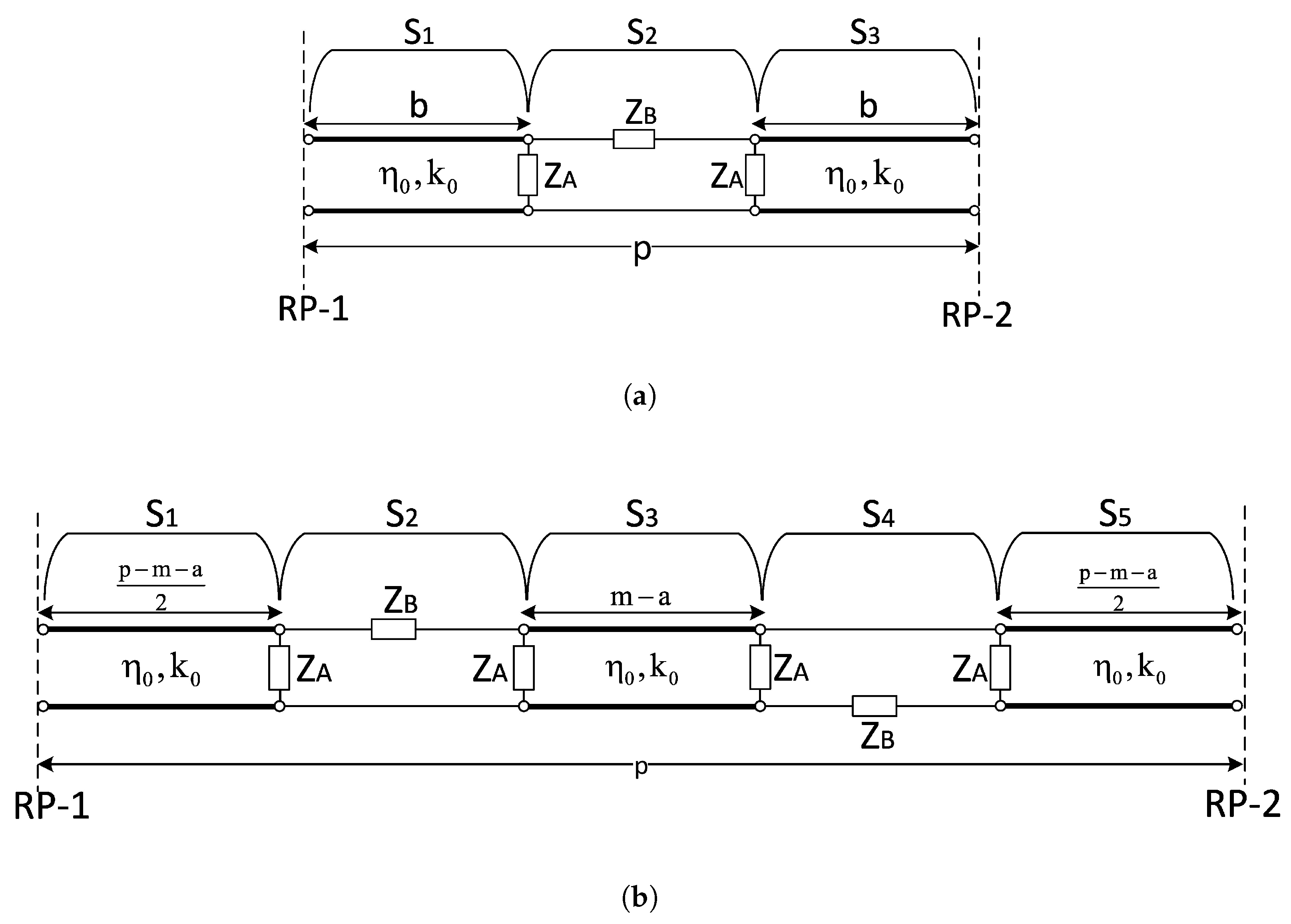
Figure 3.
and behavior for single corrugated PPW with (a) , , , , and (b) , , , , and .
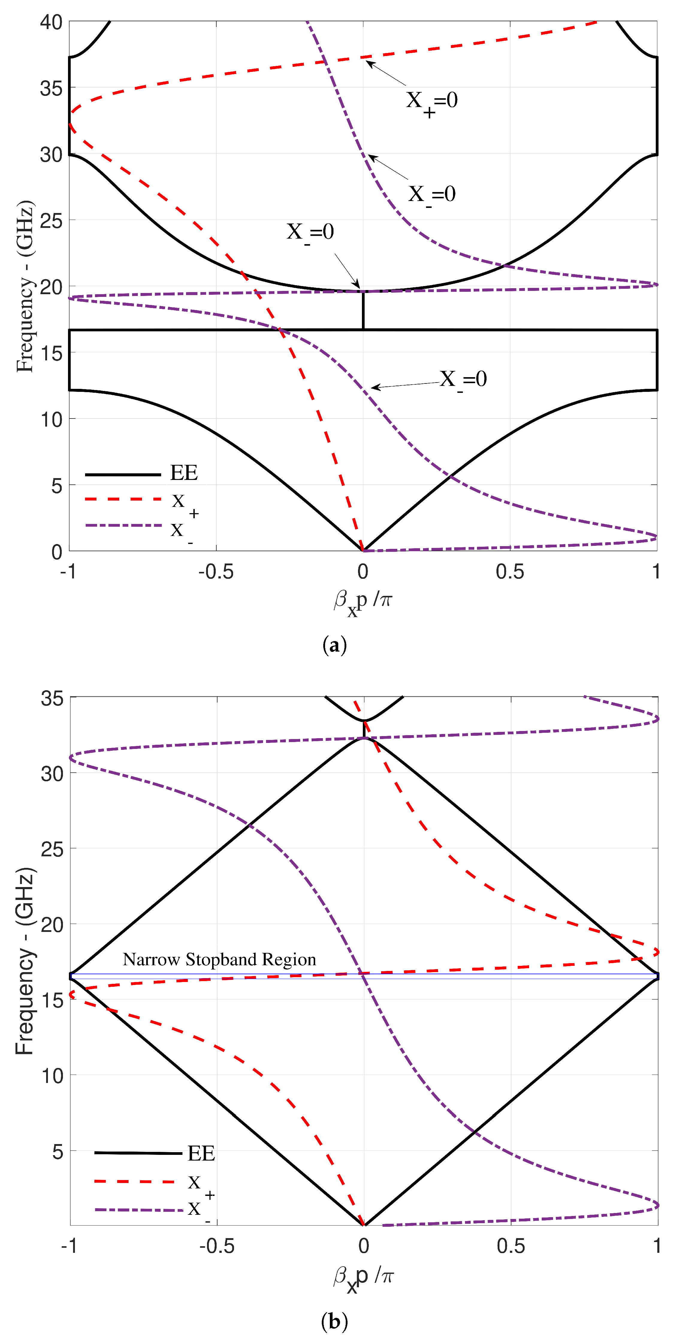
Figure 4.
and behavior for glide symmetric double corrugated PPW with (a) , , , , and (b) , , , , and .
Figure 4.
and behavior for glide symmetric double corrugated PPW with (a) , , , , and (b) , , , , and .
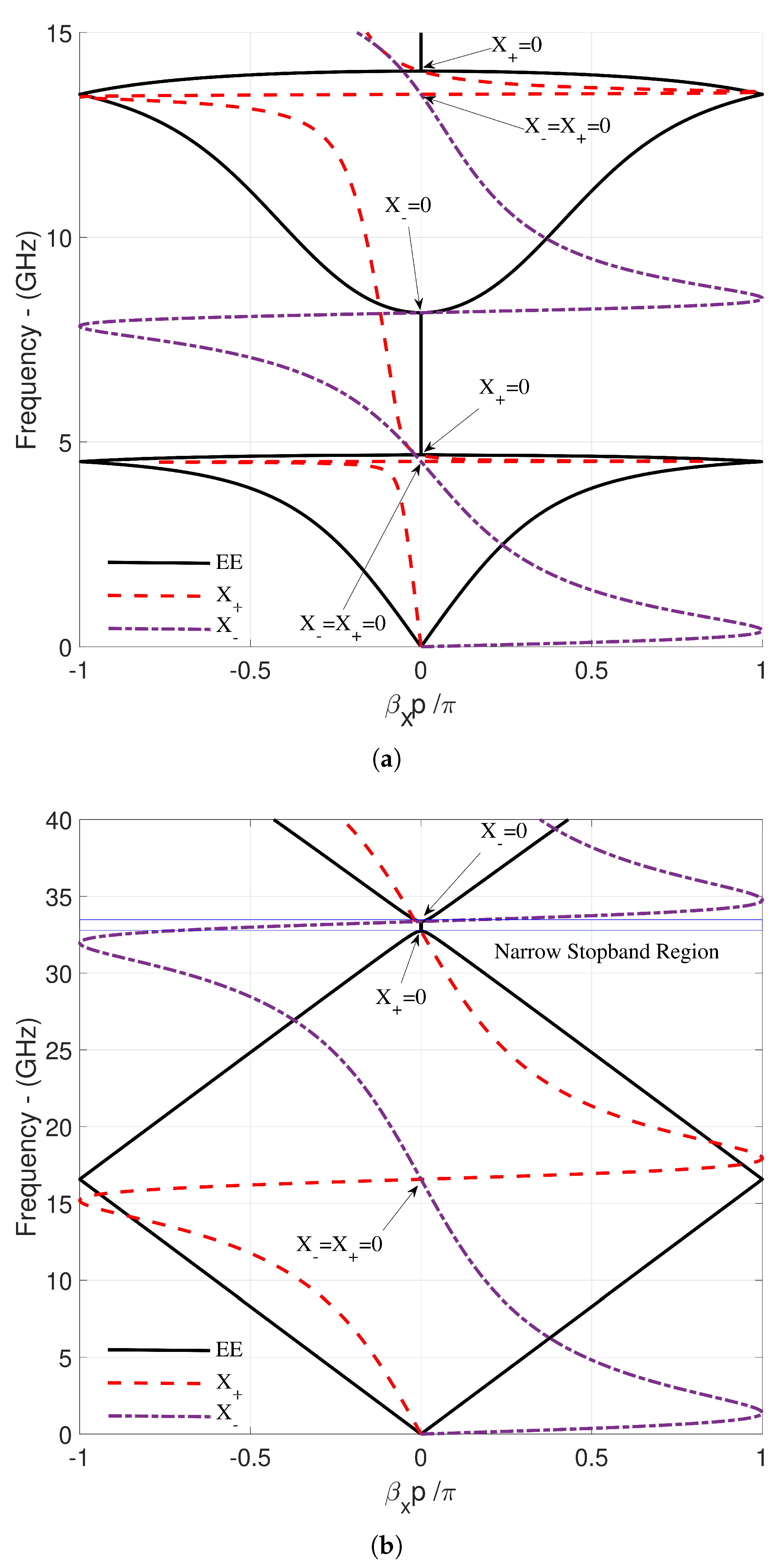
Figure 5.
Dependence of bandgap on and for , , computed via AFGSM functions and .
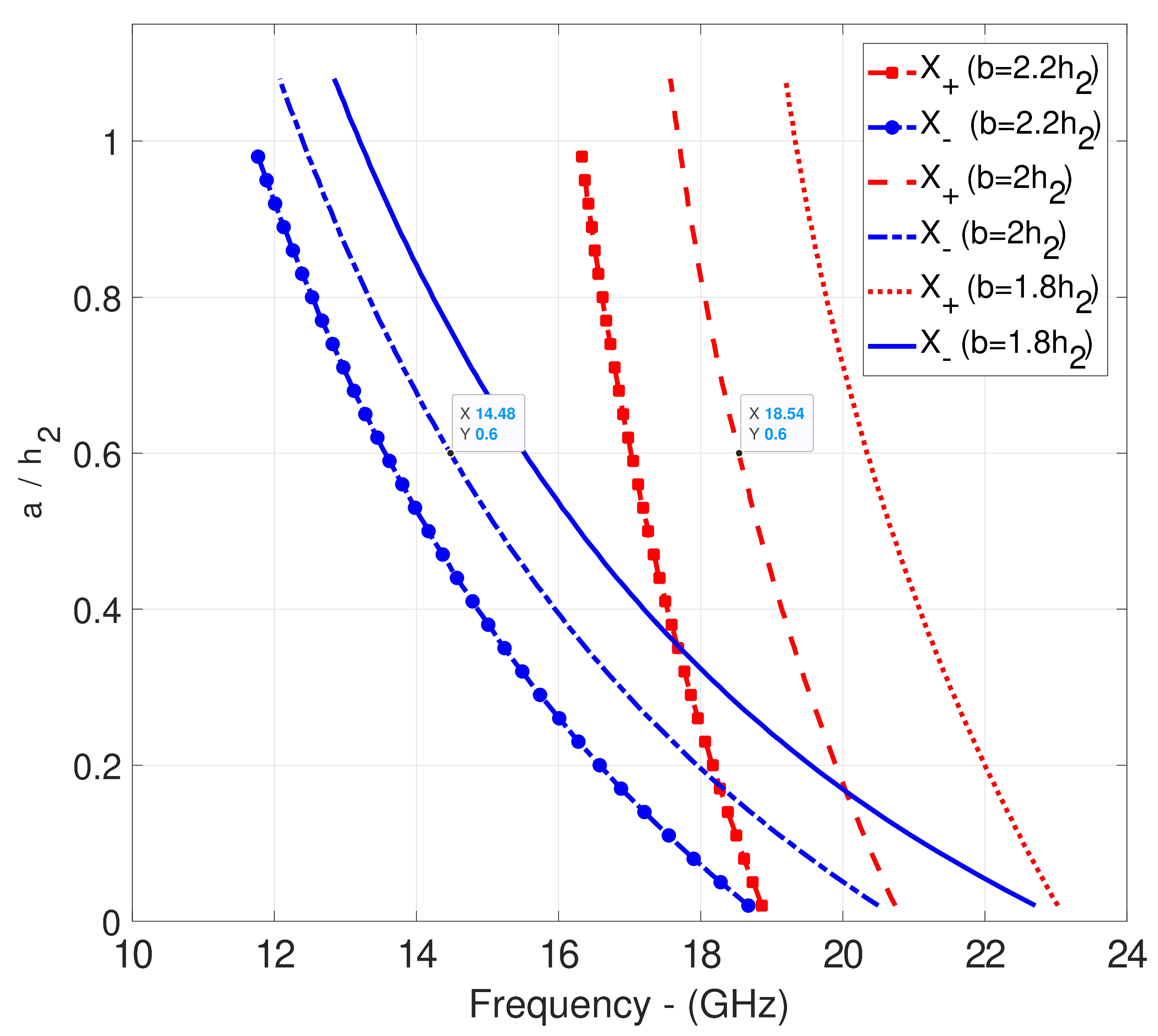
Figure 6.
(a) Designed bandgap of width , centered at . (b) Amplitude-frequency characterization of cascading different numbers of the designed single C-PPW unit cell via CST and HFSS.
Figure 6.
(a) Designed bandgap of width , centered at . (b) Amplitude-frequency characterization of cascading different numbers of the designed single C-PPW unit cell via CST and HFSS.
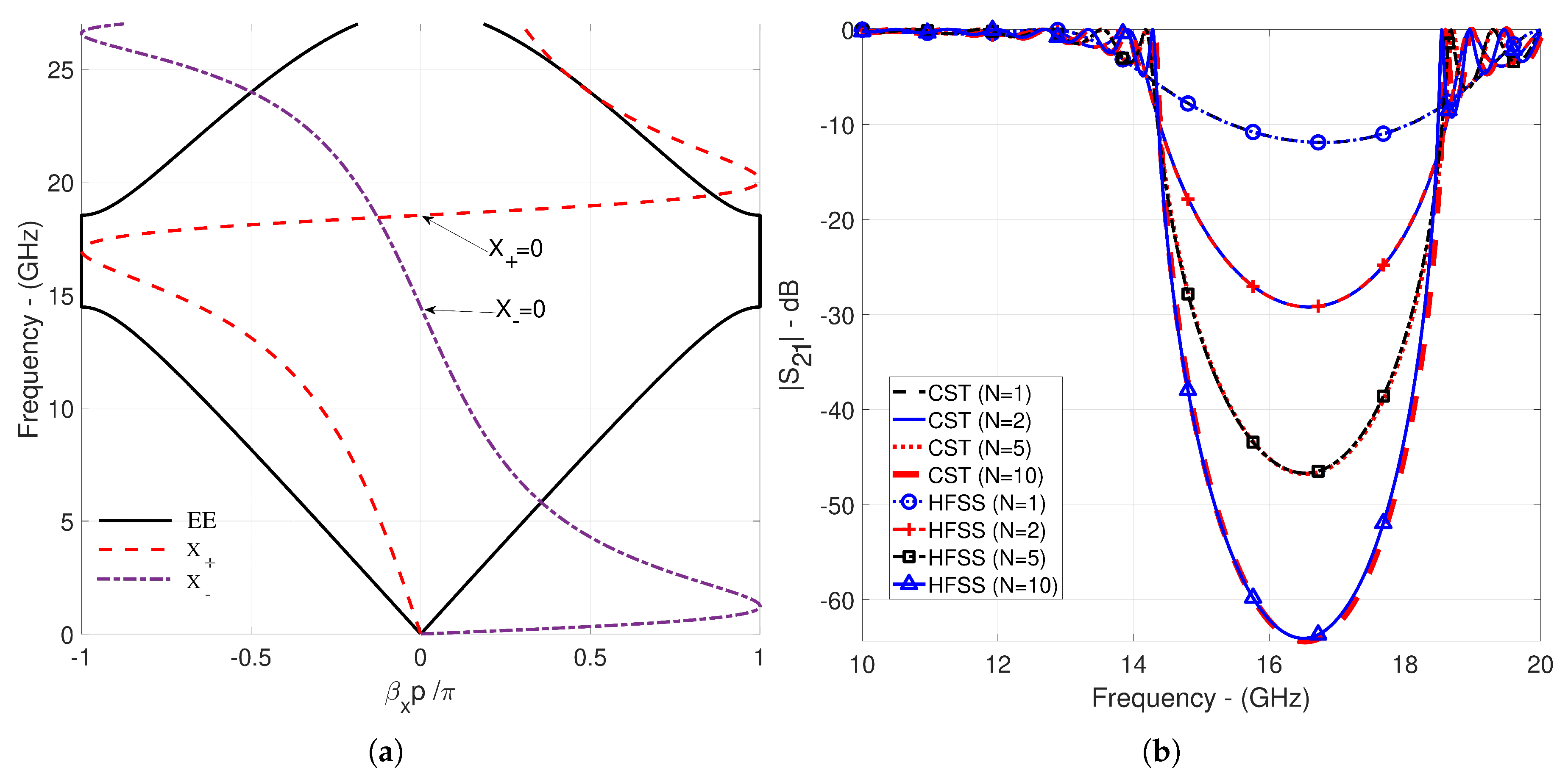
Figure 7.
(a) Obtained Passband-stopband characterization of designed glide symmetric DCPPW with AFGSM functions and other computation methods for Scenario 1. (b) -frequency characterization of cascading different numbers of the designed GS-DCPPW unit cell of Scenario 1 via CST and HFSS.
Figure 7.
(a) Obtained Passband-stopband characterization of designed glide symmetric DCPPW with AFGSM functions and other computation methods for Scenario 1. (b) -frequency characterization of cascading different numbers of the designed GS-DCPPW unit cell of Scenario 1 via CST and HFSS.
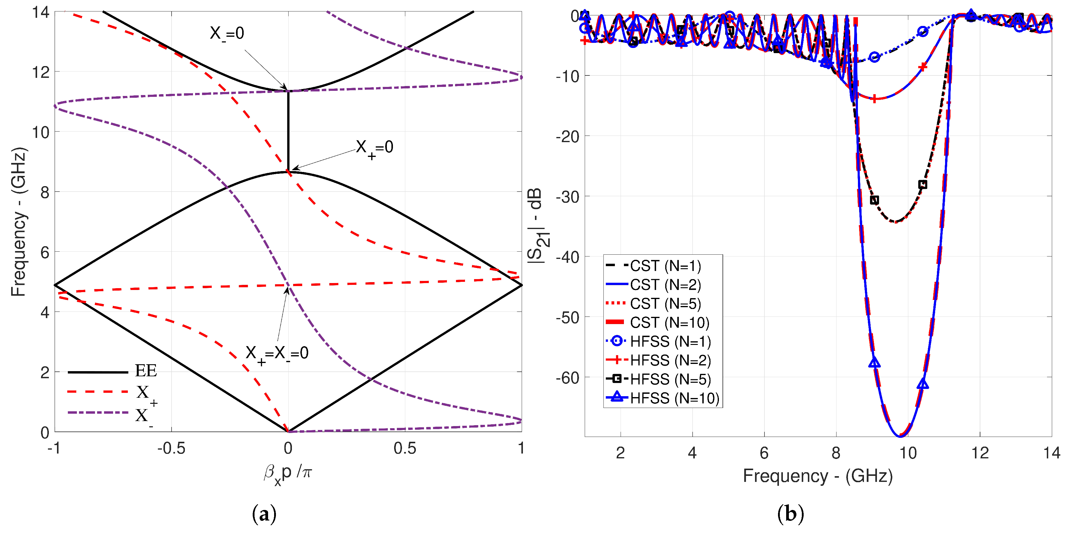
Figure 8.
(a) Obtained Passband-stopband characterization of designed glide symmetric DCPPW with AFGSM functions and other computation methods for Scenario 2. (b) -frequency characterization of cascading different numbers of the designed GS-DCPPW unit cell of Scenario 2 via CST and HFSS.
Figure 8.
(a) Obtained Passband-stopband characterization of designed glide symmetric DCPPW with AFGSM functions and other computation methods for Scenario 2. (b) -frequency characterization of cascading different numbers of the designed GS-DCPPW unit cell of Scenario 2 via CST and HFSS.
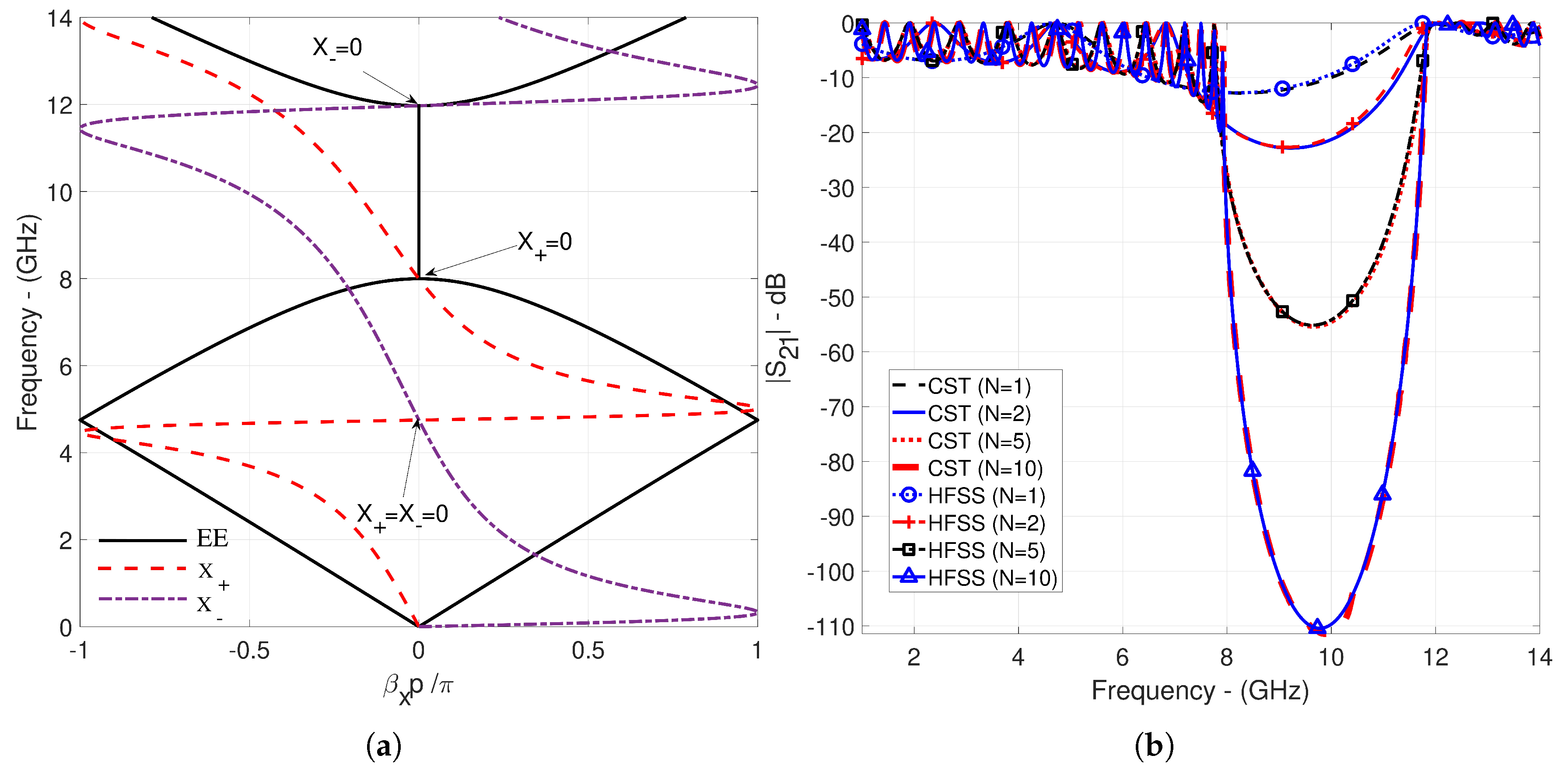
Figure 9.
(a) Obtained Passband-stopband characterization of designed glide symmetric DCPPW with AFGSM functions and other computation methods for Scenario 3. (b) -frequency characterization of cascading different numbers of the designed GS-DCPPW unit cell of Scenario 3 via CST and HFSS.
Figure 9.
(a) Obtained Passband-stopband characterization of designed glide symmetric DCPPW with AFGSM functions and other computation methods for Scenario 3. (b) -frequency characterization of cascading different numbers of the designed GS-DCPPW unit cell of Scenario 3 via CST and HFSS.
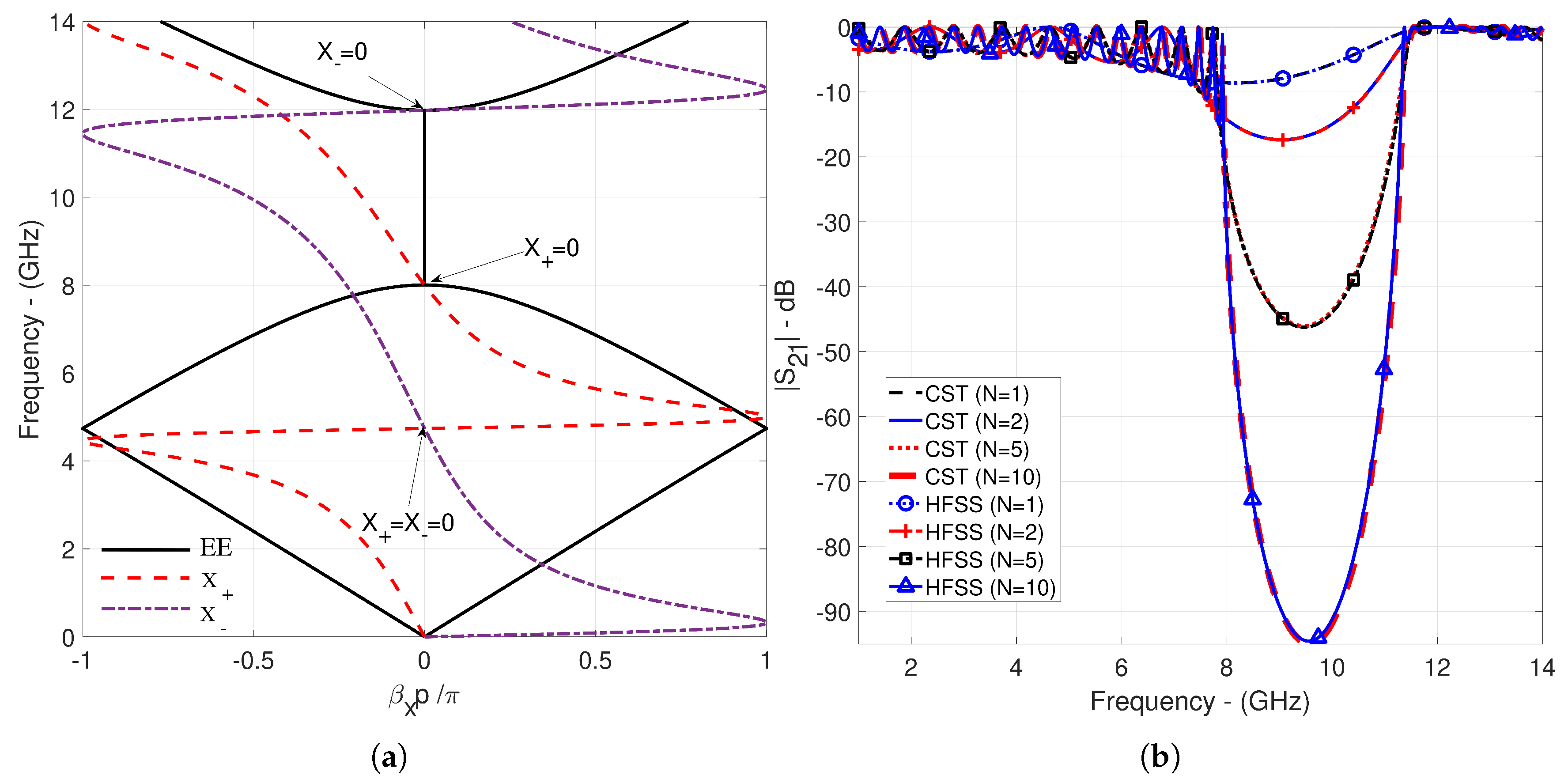
Figure 10.
Comparison of Scenario 1, Scenario 2 and Scenario 3 for obtaining design objectives.
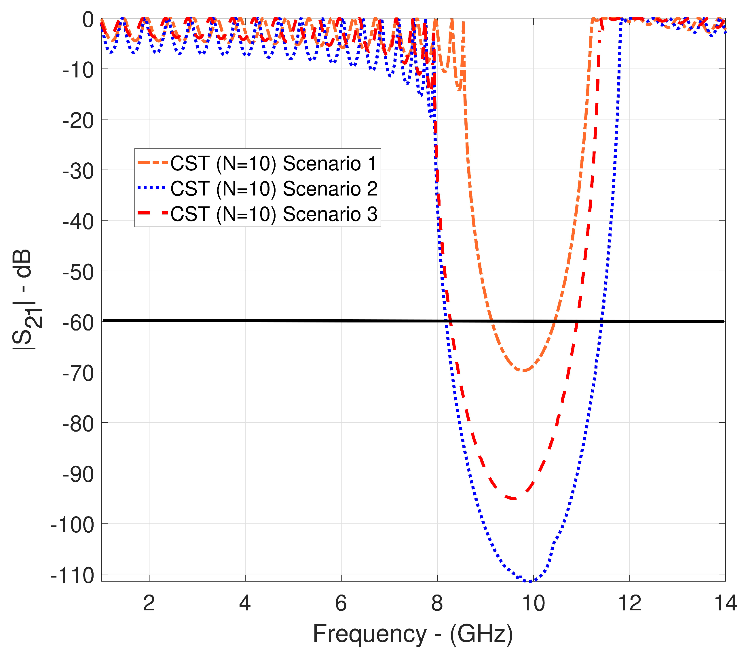

Table 1.
Band edge frequency results for the frequency behaviors of the EE and AFGSM methods in Figure 4a,b.
Table 1.
Band edge frequency results for the frequency behaviors of the EE and AFGSM methods in Figure 4a,b.
| Figures | EE | |||
|---|---|---|---|---|
| [GHz] | [GHz] | [GHz] | [GHz] | |
| Figure 4a | 4.681 | 8.157 | 4.69-8.15 | 4.52, 13.49 |
| Figure 4b | 32.729 | 33.364 | 32.73-33.363 | 16.57 |
Table 2.
Width of stopbands () centered 10GHz versus a, and b for and .
| a | b | |||
|---|---|---|---|---|
| [GHz] | [MHz] | [mm] | [mm] | [mm] |
| 1.8 | 30 | 1.1 | 1.1 | 13.6 |
| 2 | 10 | 1.2 | 1.1 | 13.5 |
| 2.7 | 10 | 1.5 | 1.2 | 13.2 |
| 1.7 | 1 | 13.3 | ||
| 3 | 10 | 1.2 | 1.8 | 12.9 |
| 3.2 | 10 | 1.5 | 1.5 | 12.9 |
| 3.6 | 10 | 1.7 | 1.5 | 12.8 |
| 2.1 | 1.1 | 13.1 | ||
| 3.8 | 10 | 1.3 | 2.2 | 12.5 |
| 1.7 | 1.6 | 12.7 | ||
| 2.2 | 1.1 | 13.1 | ||
| 4 | 20 | 1.5 | 2 | 12.5 |
| 1.9 | 1.5 | 12.7 | ||
| 2 | 1.4 | 12.8 | ||
| 2.1 | 1.3 | 12.9 | ||
| 2.2 | 1.2 | 13 | ||
| 2.3 | 1.1 | 13.1 | ||
| 4.4 | 10 | 2 | 1.6 | 12.6 |
| 10 | 2.4 | 1.2 | 13 | |
| 4.8 | 2.4 | 1.4 | 12.8 |
Table 3.
Designed unit cell parameters for all scenarios and total filter dimensions (TFD) for .
| Studies | a | b | p | TFD | |||
|---|---|---|---|---|---|---|---|
| [mm] | [mm] | [mm] | [mm] | [mm] | [mm] | [mm] | |
| Scenario 1 | 1.5 | 13.2 | 0.5 | 1.2 | 27.9 | 2.9 | 279 |
| Scenario 2 | 1.5 | 12.5 | 0.5 | 2 | 26.5 | 4.5 | 265 |
| Scenario 3 | 2.3 | 13.1 | 0.5 | 1.1 | 28.5 | 2.7 | 285 |
Table 4.
Comparison table for designed bandstop fiter via AFGSM method with literature studies.
| Works | Physical Dimensions | ||
|---|---|---|---|
| [GHz] | [GHz] | [mm × mm × mm] | |
| [3], Figure 10, MM-GSM | 9, Waveguide | @-60 dB, 0.1 | 1120.14 × 22.86 × 10.16 |
| [46], Figure 6, SONNET | 9.7, Microstrip | @ -60 dB, 1 | 12.87 × 7.04 × 0.27 |
| [47], Figure 9, Conv. BSF | 9.3, Waveguide | @ -60 dB, 1.23 | 86 × 74 × 18 |
| [47], Figure 9, Prop. BSF | 9.35, Hybrid | @ -55.5 dB, 2.67 | 15 × 8 × 1 |
| [48], Figure 10a, State (01) | 10.3, Microstrip | @ -20 dB, 0.215 | 7.3 × 7.5 × 0.508 |
| [48], Figure 10a, State (10) | 10.2, Microstrip | @ -20 dB, 0.22 | 7.3 × 7.5 × 0.508 |
| [48], Figure 14a, =25V | 9.56, Microstrip | @ -20 dB, 0.192 | 7.3 × 7.5 × 0.508 |
| [49], Table 5, Open-short | 9, Microstrip | @ -40 dB, 0.7 | 6.1 × 6.2 × 0.4 |
| Scenario 2, Figure 10, CST | 9.59, Waveguide | @-60 dB, 2.64 | 265 × 26.5 × 26.5 |
Disclaimer/Publisher’s Note: The statements, opinions and data contained in all publications are solely those of the individual author(s) and contributor(s) and not of MDPI and/or the editor(s). MDPI and/or the editor(s) disclaim responsibility for any injury to people or property resulting from any ideas, methods, instructions or products referred to in the content. |
© 2025 by the authors. Licensee MDPI, Basel, Switzerland. This article is an open access article distributed under the terms and conditions of the Creative Commons Attribution (CC BY) license (http://creativecommons.org/licenses/by/4.0/).
Copyright: This open access article is published under a Creative Commons CC BY 4.0 license, which permit the free download, distribution, and reuse, provided that the author and preprint are cited in any reuse.


