1. Introduction
With the rapid development of IoT, sensors powered by batteries are needed, so in addition to high accuracy, low power consumption is also an important requirement for delta-sigma modulators (DSM) [
1,
2,
3,
4,
5,
6,
7]. Therefore, how to balance between high accuracy and low power consumption has become the focus of exploration in the field of delta-sigma modulators.
With the popularity of the full feedforward delta-sigma topology [
8,
9,
10,
11], the summation circuit has become an important component of multi-bit DSM. Conventional summation circuits use active operational transconductance amplifiers (OTAs) as the core to sum up the signals at each node of the circuit, consuming a large amount of active power [
12,
13,
14,
15]. In order to reduce this part of power consumption, passive summation schemes have been widely adopted. However, passive summation circuits directly parallel capacitors carrying the voltage signals of each branch [
1,
16,
17,
18,
19,
20], which reduces power consumption but also causes attenuation of the summation result. This makes the design requirements for multi-bit quantizers more stringent, which is not desirable.
This paper proposes a low-power multi-bit DSM based on passive and attenuationless summation. This circuit aims to achieve coefficient multiplication of the summation through bidirectional sampling technology on the basis of conventional passive summation schemes, thereby compensating the attenuation caused by summation and achieving attenuationless summation in a passive manner. This saves active power and greatly relaxes the design requirements for multi-bit quantizers.
This paper is organized as follows:
Section 2 introduces the basic principles of conventional passive summation. The proposed passive and attenuationless summation scheme is analyzed in detail in
Section 3.
Section 4 presents a passive summation case study based on a 3-order DSM. The simulation results are shown in
Section 5 and the conclusion is drawn in
Section 6.
2. Conventional passive Summation
Conventional discrete-time DSM passive summation circuits are generally based on the principle of charge redistribution. To simplify, take the example of using passive summation to add two voltages V
ip1 and V
ip2.The working principle is shown in
Figure 1.
During Φ2, V
ip1 and V
ip2 respectively charge capacitors C
f1 and C
f2. At this time, the voltage signals carried by capacitors C
f1 and C
f2 are V
ip1 and V
ip2, respectively. During Φ1, these two voltage signals are transmitted to V
DACp for summation. Due to the parallel connection of C
f1 and C
f2, the voltage at the final summation node V
DACp will be attenuated to:
Based on the above analysis, passive summation will cause the final summation voltage to attenuate to a coefficient less than 1, which is undesirable. The attenuation of the summation coefficient will increase the design requirements of the multi-bit quantizer.
3. Proposed passive and attenuationless summation scheme
In conventional passive summation, if Cf1=Cf2 for example, only 0.5Vip1 and 0.5Vip2 are transmitted to the signal summation node VDACp, causing attenuation. To compensate for this attenuation, a simple and effective method is to increase the multiplication factor of the voltage signal carried by the capacitor. As we know, high-precision delta-sigma ADCs are often implemented in differential form, which allows the use of Vin1 (Vin2) signals that are opposite in phase to Vip1 (Vip2) for bidirectional sampling, thus achieving doubling for the summation coefficient.
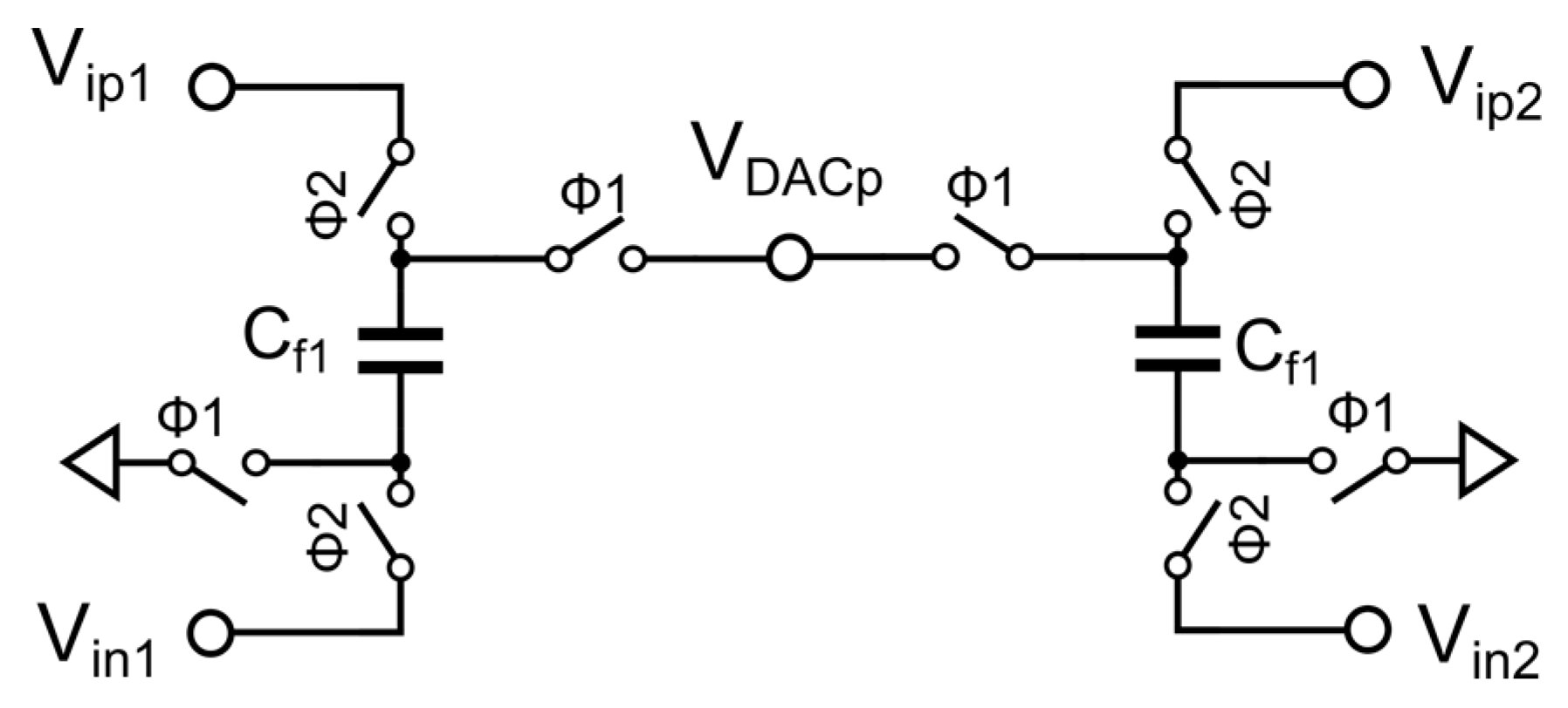
Figure 2 shows the improved bidirectional sampling passive summation scheme proposed in this paper. The timing is the same as
Figure 1(b), and the only difference from
Figure 1 is that the bottom plates of C
f1 and C
f2 are connected to V
in1 and V
in2, respectively. Through bidirectional sampling of V
ip1 and V
in1, during Φ2, the voltage carried by C
f1 is V
ip1-V
in1. Since V
ip1 and V
in1 are a pair of differential voltages, there is a relationship V
ip1-V
in1=2V
ip1, which is equivalent to the voltage signal carried by C
f1 being 2V
ip1. The same applies to C
f2. Therefore, the voltage signals carried by C
f1 and C
f2 are doubled through bidirectional sampling technology. During Φ1, these two voltage signals are transmitted to V
DACp for summation, and the voltage at the final summation node V
DACp is:
If Cf1=Cf2, then exactly 1 times the voltage signals of Vip1 and Vip2 are transmitted at the summation node. Thus, the voltage signals carried by Cf1 and Cf2 were successfully multiplied by a factor of 2 through bidirectional sampling, compensating for the attenuation caused by direct parallel connection of the summation capacitors. If a larger multiplication factor is required, a more aggressive expansion scheme can be used, such as increasing the multiplication factor by serially connecting capacitors.
Figure 3 shows the bidirectional sampling and capacitive series passive summation scheme proposed in this paper, which can achieve higher coefficient multiplication. The timing is the same as
Figure 1(b). Similar to
Figure 2, during Φ2, the sampling is completed, and the voltage signals carried by C
f1 and C
f2 are equivalent to 2V
ip1 and 2V
ip2, respectively. During Φ1, since two C
f1 capacitors are connected in series, the carried voltages are superimposed, and the series circuit composed of two C
f1 capacitors carries an equivalent voltage signal of 4V
ip1. The same applies to C
f2, so that the voltage signals carried by the summation capacitor are quadrupled through bidirectional sampling and capacitive series connection. These quadrupled voltage signals are transmitted to the summation node V
DACp for summation, and the voltage at the final summation node V
DACp is:
Similarly, if Cf1=Cf2, then at the signal summation node VDACp, twice the voltage signals of Vip1 and Vip2 are transmitted, providing the possibility to compensate for higher attenuation and increasing the applicability and flexibility of the passive and attenuationless summation scheme.
It is worth noting that this method can only series connect up to two capacitors, otherwise the parasitic capacitance of the switch will greatly affect the final summation result, and the maximum coefficient multiplication is limited to 4 and can only be an integer multiple. In conventional passive summation, the attenuation increases as the number of summation paths increases, making this scheme less attractive. However, fortunately, in DSMs, the number of summation paths does not exceed 4, and the sum of the summation coefficients (attenuation) is also smaller than this value. Using dynamic-range scaling technology to design summation coefficients as digital numbers such as 0.25、0.5、1 and 2 can help the summation capacitor arrays achieve better matching. In addition, we can parallel additional capacitors to ground at the summation node to control the attenuation value, making it easy to round off the attenuation to an integer.
For DSMs with a summation coefficient sum ≤ 2, it can use bidirectional summation alone to compensate for the attenuation. With a coefficient sum ≤ 4, it need to use the bidirectional sampling and capacitive series connection scheme with greater coefficient multiplication. With a coefficient sum > 4, we can first try to reduce the coefficient sum by loop coefficient scaling or reducing the summation path. If we cannot reduce the summation coefficients, although we cannot compensate for attenuation perfectly, we can try to suppress this attenuation as much as possible.
4. Design example based on passive and attenuationless summation scheme
To verify the reliability of the passive and attenuationless summation scheme, we designed a 3-order DSM based on 4-bit quantizer. This case is significant because the third order is implemented in a passive manner, reducing the number of summation paths and making the proposed scheme even more attractive.
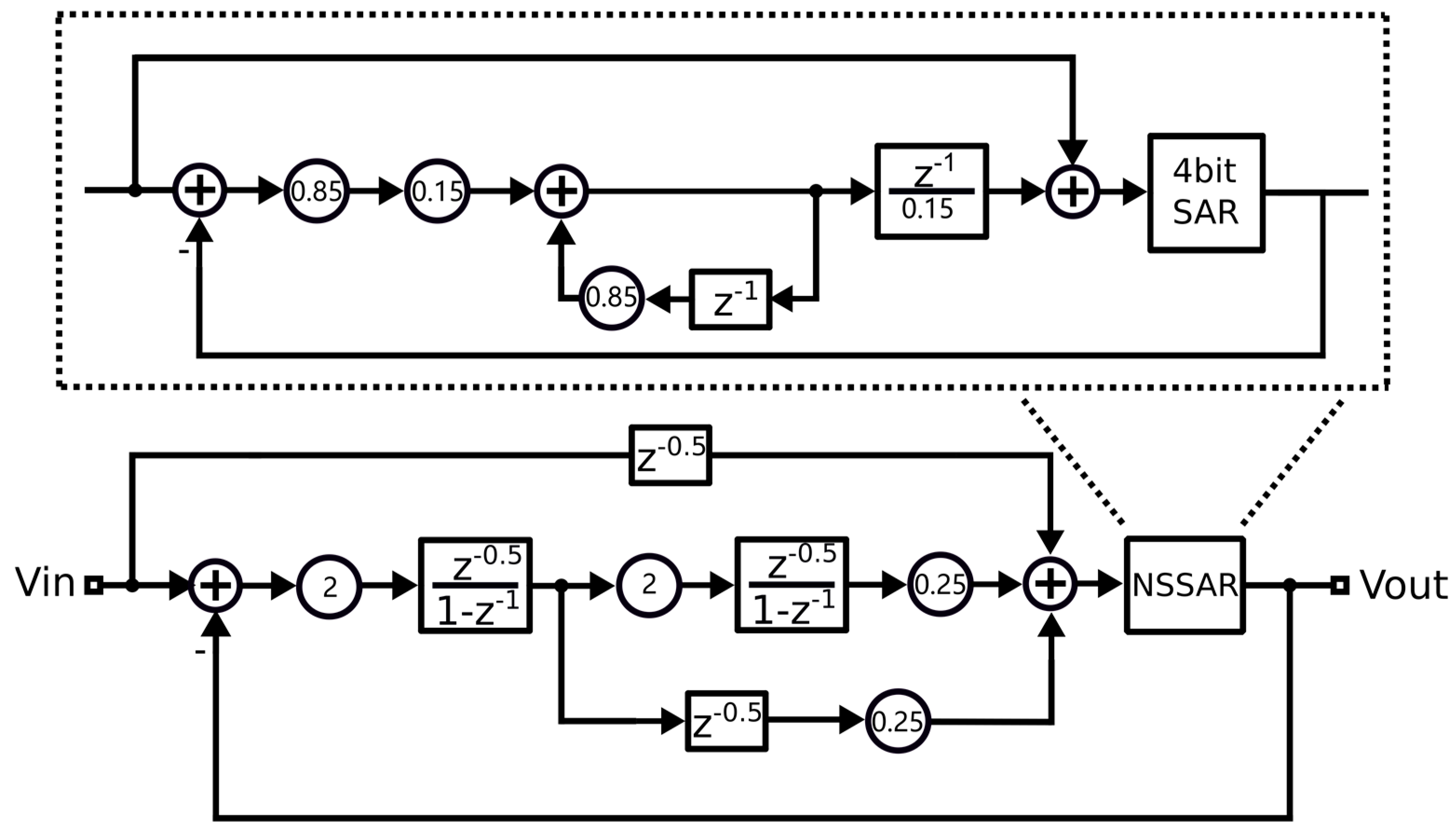
Figure 4 shows the system block diagram of a low-power multi-bit DSM based on passive and attenuationless summation. The system cascades a 1-order loop based on 4-bit NSSAR quantizer [
21,
22,
23,
24,
25] with a 2-order CIFF modulator structure to achieve the 3-order loop in a passive manner, further reducing the total power consumption of the system. The noise transfer function of the entire system is designed as follows:
In this system, there are three summation paths and the sum of the summation coefficients is 1.5 < 2, so we can use bidirectional summation alone to compensate for the attenuation.
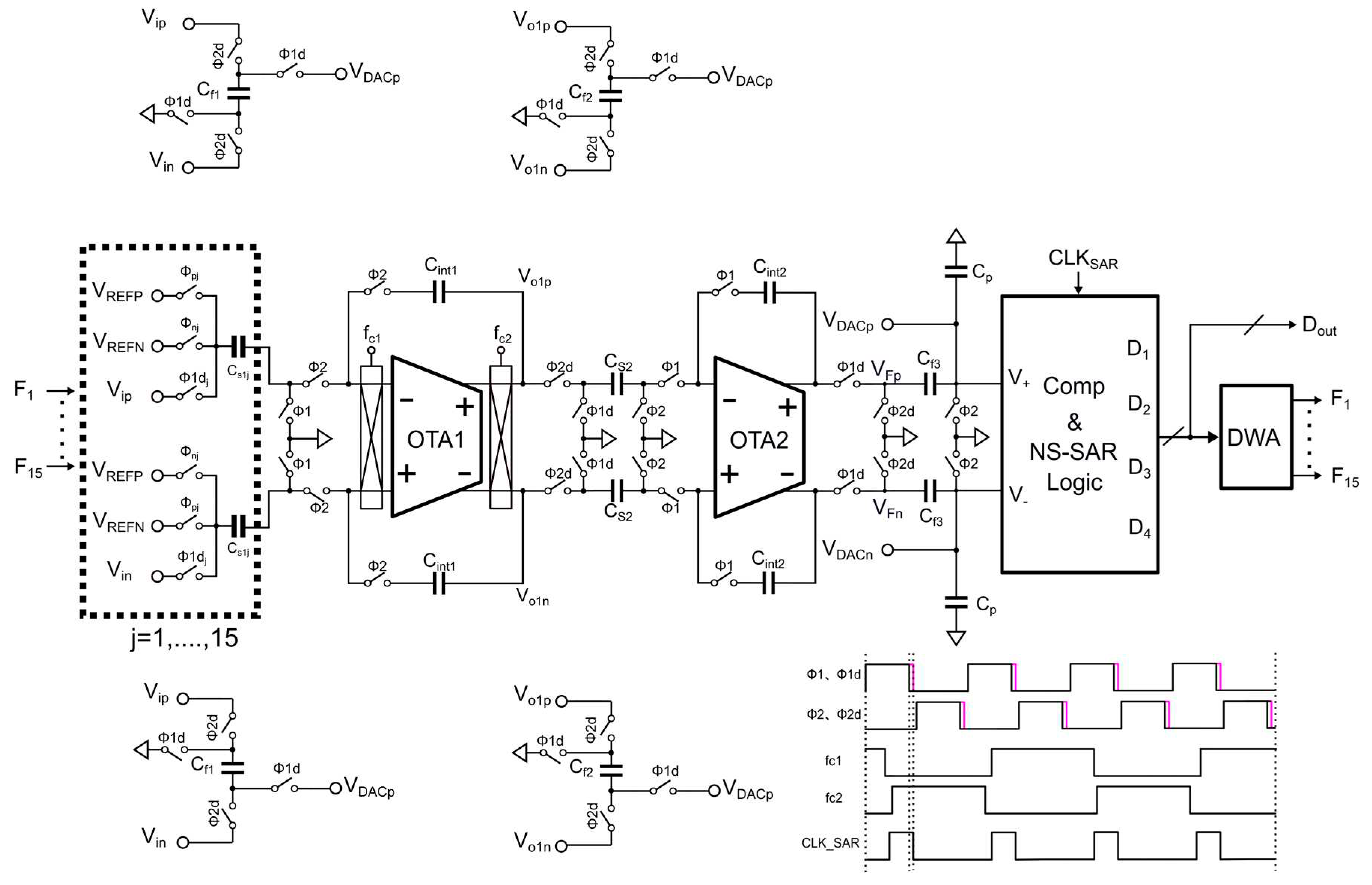
Figure 5 shows the circuit and timing diagram of the low-power multi-bit DSM based on passive and attenuationless summation. The circuit consists of two integrators, passive summation circuits, 4-bit NSSAR quantizer, DWA module, and feedback DAC arrays. The OTA in the integrator is chosen as the FIA structure [
17,
26,
27,
28,
29,
30], further improving the energy efficiency advantage of this DSM. It should be noted that the summation circuit completes the passive and attenuationless summation through bidirectional sampling. The signals to be summed by the summation circuit are V
ip-V
in, V
o1p-V
o1n, and V
o2p-V
o2n, and the required summation coefficients are 1:0.25:0.25. During Φ2d, the input signal and OTA1 charge the positive terminals C
f1 and C
f2 through bidirectional sampling technology, causing the voltage carried by C
f1 and C
f2 to be equivalent to 2 times V
ip and V
o1p, achieving a coefficient doubling. Additionally, the voltage of C
f3 is cleared. During Φ1d, the voltage of the positive terminals C
f1 and C
f2 is pushed to the summing node V
DACp for summation. At the same time, OTA2 charges C
f3. The same applies to the negative terminal V
DACn. The final summing node V
DACp-V
DACn is:
Where C
p is the estimated parasitic capacitance. If C
f1:C
f2:C
f3:C
p=4:1:2:1, then the final V
DACp-V
DACn is:
Therefore, by using bidirectional sampling technology to achieve coefficient doubling for the voltage signals carried by Cf1 and Cf2, a passive and attenuationless summation method is achieved.
5. The simulation results
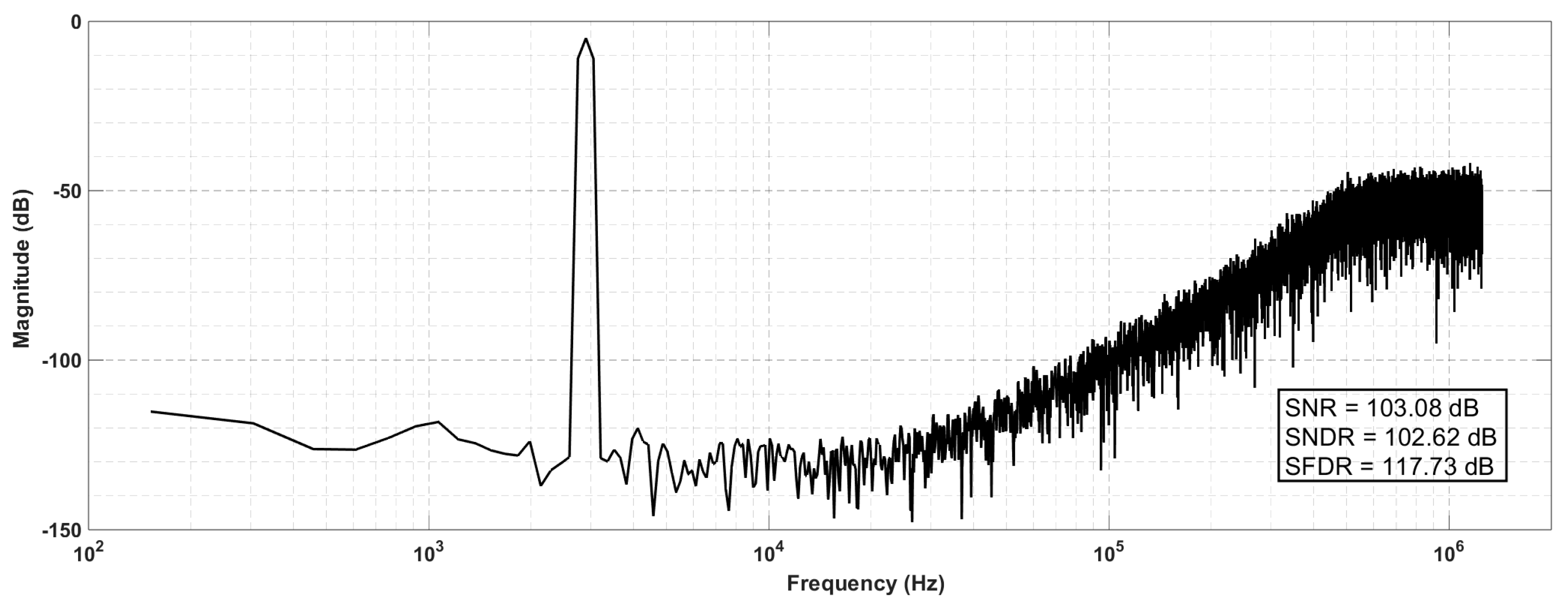
This DSM based on passive and attenuationless summation was designed using the 180nm CMOS process. The DSM runs at 2.5 MHz with a 1.2V supply. Under an input signal of 2.9 kHz, the 4-bit code stream output by the modulator was analyzed as shown in
Figure 6. In a bandwidth of 20 kHz, the simulated SNR, SNDR and SFDR are 103.08 dB, 102.62 dB and 117.73 dB. The total power consumption is 148.32 μW, with analog power consumption at 78 μW and digital power consumption at 70.32 μW.
6. The simulation results
This paper proposes a low-power multi-bit DSM based on passive and attenuationless summation. By using bidirectional sampling and capacitor series connection, the voltage signals carried by the summation circuit are multiplied, successfully compensating for the attenuation caused by the parallel connection of the summation capacitors and greatly relaxing the design requirements of the subsequent multi-bit quantizer. Moreover, this scheme does not introduce additional active overhead. The validation case of a 3-order DSM based on 4-bit quantizer in the 180nm CMOS process demonstrates good performance in simulation results. The design case used provides a new approach to reduce passive summation paths, making the proposed passive and attenuationless summation scheme highly advantageous in multi-bit DSMs design.
Author Contributions
Rongshan Wei: Conceptualization, Methodology, Software. Lijie Huang: Data curation, Writing- Original draft preparation. Gongxing Huang: Conceptualization, Methodology. Renping Wang: Visualization, Investigation. Cong Wei: Methodology, Reviewing.
Funding
This work was supported by the Natural Science Foundation of Fujian Province, China (Grant No. 2023J01398)..
Conflicts of Interest
The authors declare no conflict of interest.
References
- Y. Chae.; G. Han. Low Voltage, Low Power, Inverter-Based Switched-Capacitor Delta-Sigma Modulator. IEEE Journal of Solid-State Circuits. 2009, 44, 458-472. [CrossRef]
- Je-Kwang Cho. Low-power sigma-delta modulator with half-sample delayed-input feedforward. IEICE Electronics Express. 2014, 11, 1349-2543. [CrossRef]
- D. Laouej.; H. Daoud.; M. Loulou. A Very Low Power Delta Sigma Modulator Using Optimized Bulk Driven Telescopic OTA for Biomedical Devices. In 2020 IEEE International Conference on Design & Test of Integrated Micro & Nano-Systems (DTS), Hammamet, Tunisia, 2020, pp. 1-6. [CrossRef]
- J. Kim.; H. Shin.; S. Na. A 860.8-nW Low-Power Continuous-Time Delta-Sigma Modulator With Switched Resistors for Sensor Applications. In 2023 IEEE International Symposium on Circuits and Systems (ISCAS), Monterey, CA, USA, 2023, pp. 1-5. [CrossRef]
- B. Zhao.; Y. Lian.; A. M. Niknejad. A Low-Power Compact IEEE 802.15.6 Compatible Human Body Communication Transceiver With Digital Sigma-Delta IIR Mask Shaping. IEEE Journal of Solid-State Circuits. 2019, 54, 346-357. [CrossRef]
- T. -C. Wang.; Y. -H. Lin. A 0.022 mm2 98.5 dB SNDR Hybrid Audio ΔΣ Modulator With Digital ELD Compensation in 28 nm CMOS. IEEE Journal of Solid-State Circuits. 2015, 50, 2655-2664. [CrossRef]
- M. Jang.; C. Lee. Analysis and Design of Low-Power Continuous-Time Delta-Sigma Modulator Using Negative-R Assisted Integrator. IEEE Journal of Solid-State Circuits. 2019, 54 , 277-287. [CrossRef]
- J.Silva.; U. Moon. Wideband low-distortion delta-sigma ADC topology. Electron. Lett.. 2001, 37, 737-738. [CrossRef]
- M. A. Mokhtar.; P. Vogelmann.; J. Wagner. Incremental Sturdy-MASH Sigma-Delta Modulator with Reduced Sensitivity to DAC Mismatch. In 2019 IEEE International Symposium on Circuits and Systems (ISCAS), Sapporo, Japan, 2019, pp. 1-5. [CrossRef]
- P. P. Bora.; D. Borggreve.; F. Vanselow. A 0.8 V Low-Power 3rd order Sigma-Delta Modulator in 22 nm FDSOI CMOS Process for Sensor Interfaces. In 2019 17th IEEE International New Circuits and Systems Conference (NEWCAS), Munich, Germany, 2019, pp. 1-4. [CrossRef]
- H. Park.; K. Nam. A 0.7-V 870-μ W Digital-Audio CMOS Sigma-Delta Modulator. IEEE Journal of Solid-State Circuits. 2009, 44, 1078-1088. [CrossRef]
- Y.Tang.; S.Gupta.; J. Paramesh. A digital-summingfeedforward Σ−∆ modulator and its application to a cascade ADC. In TheProceedings of the IEEEInternational Symposium of Circuits and Systems(ISCAS ), New Orleans, USA, May 2007, pp. 485-488. [CrossRef]
- Y. Ye.; L. Liu.; J. Li. A 120dB SNDR audio sigma-delta modulator with an asynchronous SAR quantizer. In 2012 IEEE International Symposium on Circuits and Systems (ISCAS), Seoul, Korea (South), 2012, pp. 2357-2360. [CrossRef]
- S. Mehrotra.; E.Eland.; S. Karmakar. A 590 µW, 106.6 dB SNDR, 24 kHz BW Continuous-Time Zoom ADC with a Noise-Shaping 4-bit SAR ADC. In ESSCIRC 2022- IEEE 48th European Solid State Circuits Conference (ESSCIRC), Milan, Italy, 2022, pp. 253-256. [CrossRef]
- E. Eland.; S. Karmakar. A 440-μW, 109.8-dB DR, 106.5-dB SNDR Discrete-Time Zoom ADC With a 20-kHz BW. IEEE Journal of Solid-State Circuits. 2021, 56, 1207-1215. [CrossRef]
- Y. Tang.; X. Chen.; H Zhu. A 108-dB SNDR 2–1 MASH ΔΣ Modulator with First-Stage Multibit for Audio Application. In 2018 IEEE 3rd International Conference on Integrated Circuits and Microsystems (ICICM), Shanghai, China, 2018, pp. 336-340. [CrossRef]
- R. S. A. Kumar.; N. Krishnapura. Analysis and Design of a Discrete-Time Delta-Sigma Modulator Using a Cascoded Floating-Inverter-Based Dynamic Amplifier. IEEE Journal of Solid-State Circuits, 2022, 57, 3384-3395. [CrossRef]
- M. Zhao.; Y. Zhao. A 4-μW Bandwidth/Power Scalable Delta–Sigma Modulator Based on Swing-Enhanced Floating Inverter Amplifiers. IEEE Journal of Solid-State Circuits. 2022, 57, 709-718. [CrossRef]
- J. -S. Huang.; S. -C. Kuo. A Multistep Multistage Fifth-Order Incremental Delta Sigma Analog-to-Digital Converter for Sensor Interfaces. IEEE Journal of Solid-State Circuits. 2023, 58, 2733-2744. [CrossRef]
- Jinho Noh.; Jisoo Lee. An analog sigma-delta modulator with shared operational amplifier for low-power class-D audio amplifier. IEICE Electronics Express. 2015, 12, 1349-2543. [CrossRef]
- H. Zhuang.; W. Guo. A Second-Order Noise-Shaping SAR ADC With Passive Integrator and Tri-Level Voting. IEEE Journal of Solid-State Circuits. 2019, 54, 1636-1647. [CrossRef]
- S. Li.; B. Qiao. A 13-ENOB Second-Order Noise-Shaping SAR ADC Realizing Optimized NTF Zeros Using the Error-Feedback Structure. IEEE Journal of Solid-State Circuits. 2018, 53, 3484-3496. [CrossRef]
- H. Hu.; V. Vesely.; U. -K. Moon. Ultra-Low OSR Calibration Free MASH Noise Shaping SAR ADC. In 2022 IEEE International Symposium on Circuits and Systems (ISCAS), Austin, TX, USA, 2022, pp. 1244-1248. [CrossRef]
- A. Aprile.; M. Folz.; D. Gardino. A 0.06-mm2 Current-Mode Noise-Shaping SAR based Temperature-to-Digital Converter with a 4.9-nJ Energy/Conversion. In 2023 IEEE Custom Integrated Circuits Conference (CICC), San Antonio, TX, USA, 2023, pp. 1-2. [CrossRef]
- K. Li.; S. -W. Sin.; L. Qi. A Robust Hybrid CT/DT 0-2 MASH DSM with Passive Noise-Shaping SAR ADC. In 2022 IEEE International Symposium on Circuits and Systems (ISCAS), Austin, TX, USA, 2022, pp. 551-555. [CrossRef]
- X. Tang.; L. Shen. An Energy-Efficient Comparator With Dynamic Floating Inverter Amplifier. IEEE Journal of Solid-State Circuit. 2020, 55, 1011-1022. [CrossRef]
- Y. Hu.; Y. Zhao.; W. Qu. A 2.87μW 1kHz-BW 94.0dB-SNDR 2-0 MASH ADC Using FIA with Dynamic-Body-Biasing Assisted CLS Technique. In 2022 IEEE International Solid- State Circuits Conference (ISSCC), San Francisco, CA, USA, 2022, pp. 410-412. [CrossRef]
- X. Hao.; J. Chen.; L. Meng. A 94.6dB-SNDR 50kHz-BW 1-1-1 MASH ADC Using OTA-FIA Based Integrators. In 2023 IEEE International Symposium on Circuits and Systems (ISCAS), Monterey, CA, USA, 2023, pp. 1-4. [CrossRef]
- X. Wu.; Y. Liu.; H. Lu. A 77.2-dB SNDR SAR ADC With a Segmented Comparator Logic Based on Compensatory SA Latch for FIA. In 2021 IEEE MTT-S International Wireless Symposium (IWS), Nanjing, China, 2021, pp. 1-3. [CrossRef]
- H. Li.; Z. Tan. Energy-Efficient CMOS Humidity Sensors Using Adaptive Range-Shift Zoom CDC and Power-Aware Floating Inverter Amplifier Array. IEEE Journal of Solid-State Circuits. 2021, 56, 3560-3572. [CrossRef]
|
Disclaimer/Publisher’s Note: The statements, opinions and data contained in all publications are solely those of the individual author(s) and contributor(s) and not of MDPI and/or the editor(s). MDPI and/or the editor(s) disclaim responsibility for any injury to people or property resulting from any ideas, methods, instructions or products referred to in the content. |
© 2023 by the authors. Licensee MDPI, Basel, Switzerland. This article is an open access article distributed under the terms and conditions of the Creative Commons Attribution (CC BY) license (http://creativecommons.org/licenses/by/4.0/).


