1. Introduction
Periodically pulsed sources of powerful coherent mid-infrared (mid-IR) radiation have a wide range of applications in many areas of science and technology. In particular, frequency converters operating in the 3.5-5 μm and 8-μm wavelength ranges are promising for optical communications in the atmosphere within the framework of global 6G-generation information transmission systems [
1]. Sources of coherent mid-IR radiation are also used for processing materials (glasses, ceramics, or semiconductors) by scribing and thermal splitting [
2,
3], in medicine, including disease diagnosis using gas analysis and resonant ablation of biological tissues due to the strong water and collagen absorptions [
4,
5,
6]. Sources of coherent radiation capable of generating powerful pulsed radiation in the 3.5-5 μm wavelength range are relevant for the creation of lidar systems based on the method of differential absorption for greenhouse gas emission control (since the most intense absorption lines of most greenhouse gases lie in this spectral range) [
7,
8,
9]. One of the most efficient solid-state sources of coherent radiation in the mid-IR range are optical parametric oscillators (OPOs) and optical parametric generators (OPGs).
The most powerful OPOs and OPGs in the wavelength range of 3.5-5 μm are currently based on nonlinear-optical ZnGeP
2 (ZGP) crystals [
10]. These OPOs are capable of generating radiation with an average power of up to 160 W or pulse energy of up to 200 mJ at a pulse duration of 20-60 ns and a repetition rate of from units of Hz to 100 kHz [
11,
12,
13]. However, the long-term operation without failure of powerful OPOs and OPGs based on ZGP is limited by laser-induced damage (LID) of the surface of this material. In this regard, the potential for practical use of these OPOs in the mid-IR range is associated, in particular, with the need to improve the methods of synthesis, growth, and processing of the working surfaces of crystals in order to increase the LID threshold (LIDT).
There have been a number of publications on the problem of the ZGP LID by the laser irradiations at wavelengths from 1.064 μm to 10 μm [
14,
15,
16,
17,
18,
19,
20,
21]. These studies have revealed a significant difference in the optical breakdown threshold of the ZGP crystal at wavelengths of 1.064 μm and 2.1 μm [
14]. Dynamic visualization of the breakdown process by laser radiation at a wavelength of 2.1 μm in the ZGP volume showed that optical breakdown of the ZGP single crystal is initiated by thermal effects [
15]. The increase in the ZGP LIDT with a decrease in the pulse width of the pump radiation reported in [
16] also “supports the thermal nature of the breakdown for nanosecond pulses due to anomalous infrared absorption.” In [
18], it was reported that the ZGP LIDT at 9.55 μm was determined by the intensity of the incident beam of 142 MW/cm2 at a pulse duration of 85 ns and a repetition rate of 1 Hz, which is ~ 9.5 J/cm
2 in terms of the pulse energy density. A direct dependence of the LIDT on the growth technology and optical quality of crystals was demonstrated in [
17].
In [
22], it was shown that the LIDTs measured for the ZGP samples with aa anti-reflection (AR) coating are much lower than for samples without a coating. In [
20], it was shown that the application of the AR interference coatings leads to a twofold increase in the LIDT. In [
23], it is directly concluded that, in order to increase the output power and efficiency of parametric frequency conversion in the ZGP crystal in the spectral range of 3-5 μm, further research should be focused on improving the quality of the AR coating using a high-quality ZGP crystal.
The conflicting information about the effect of interference coatings on the ZGP LIDT presented in [
20,
22] suggests that the different design of coatings and methods of their application to a nonlinear crystal significantly affects the efficiency of its use in OPOs. In [
24,
25,
26,
27], comprehensive studies were conducted on the influence of the parameters of application of AR coatings and film-forming materials on the ZGP LIDT under the mid-IR laser irradiation with femtosecond, picosecond, and nanosecond pulse durations.
In [
17,
20] it was shown that improving the polishing of ZGP working surfaces and reducing or completely removing the near-surface crack layer leads to an increase in the LIDT. In [
20] when the near-surface crack layer was reduced, Rq was reduced by half and the PV parameter changed by more than 5 times, the optical breakdown threshold by energy density increased 2 times. LIDT at a wavelength of 2.05 μm and a pulse repetition frequency (PRR) of 10 kHz for ZGP samples with a deposited antireflection coating was improved from 1 J/cm
2 to 2 J/cm
2. The increase in LIDT was achieved by improving the polishing of the surface of ZGP samples. At the same time, the research results presented in [
17] show that with almost unchanged polishing parameter Rz, but with variation of the Rq parameter by more than four times and variation of the Ra parameter by more than 5 times, no changes in LIDT were observed. It was suggested that it is the roughness of the polished surface (peaks and valleys), described by the Rz parameter, that contributes to the mechanism of optical breakdown and can be “seeding” inhomogeneities for the initiation of optical breakdown due to field effects at a wavelength of 2091 nm.
One of the promising methods for improving surface quality is magnetorheological polishing [
28], which is increasingly being used in the processing of laser crystals to improve the threshold of radiation resistance and reduce the level of roughness. In [
29], magnetorheological processing was first used for polishing the working surfaces of a ZGP single crystal, in which a non-aqueous liquid with magnetic particles of carbonyl iron with the addition of nanodiamonds was used. Samples of a ZGP single crystal with a surface roughness level in angstroms were obtained. The use of magnetorheological polishing made it possible to more accurately characterize possible structural defects that arose on the surface of the single crystal and had a size of ~0.5–1.5 μm. The value of the LIDT caused by the laser at the specified surface roughness parameters was determined not by the quality of polishing, but by the number of point recesses caused by physical limitations of the structural configuration of the crystal volume. These results are in good agreement with the assumption about the significant influence of the dislocation concentration in the ZGP crystal on LIDT put forward in [
30]. Despite the fact that the sample subjected to MRP showed a significant improvement in the surface roughness parameters compared to the sample polished using traditional technology, LIDT practically did not change. The absence of a difference in the LIDT for the two samples was due to the physical limitations of the structural configuration of the crystal.
Based on the data provided in
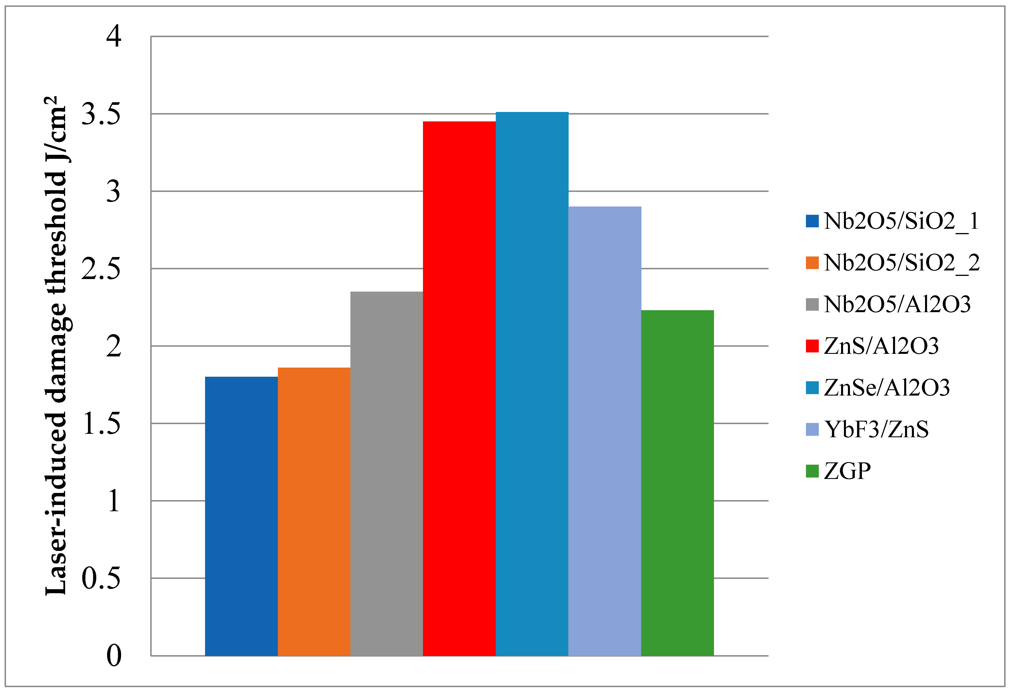
Table 1, it can be seen that the LIDT can be affected by the structural perfection and impurity composition of the crystal, the quality of the crystal's working surfaces, as well as the influence of external factors (parameters of the testing laser radiation, crystal temperature). Further, in this paper, an overview of the results of determining the contribution to the value of LIDT of each of the factors listed above will be presented. The tested ZGP samples were manufactured by “LOC” Ent., Tomsk, Russia, or Harbin Institute of Technology (HIT), Harbin, China. The single-crystaline ZGP samples had the high purity and structural perfection [
17,
30]. The repertitevely-pulsed Ho
3+:YAG lasers at 2097 nm pumped by a Tm fiber laser at 1908 nm were used for the LID tests [
31]. The "R-on-1" method was applied for all ZGP LIDT tests [
32].
2. The effect of the defect structure of the ZGP crystal lattice on the LIDT value
The effect of the ZGP structure on the LIDT was tested in the first series for the samples manufactured by Harbin Institute of Technology. The first tested element with dimensions of 6×6×20 mm3 was cut from a ZGP crystal grown in the year 2012 (samples N1). The axis of the samples N1 element was oriented at angles of Ө = 57.20 and ϕ = 00 with respect to crystal optical axis.
The second tested elements with dimensions of 6×6×3 mm3 (2 plates) were cut from a novel ZGP crystal grown in 2020 year (samples N2). The samples N2 elements was cut at angles Ө = 57.20 and ϕ = 00 with respect to the crystal optical axis.
The ZGP crystals, samples N1 and samples N2, were grown under different technological parameters: the growth rate was 0.8 mm/h and 0.3 mm/h, the temperature gradient was 9.0 K/cm and 5.0 K/cm for samples N1 and samples N2 ZGP crystals, respectively. The different growth parameters resulted in a difference of LIDT of the ZGP crystals. In our previous reports, the main types of defects detected by X-ray topography in ZGP were macroscopic stress fields, dislocations, growth striae, and microdefects [
33,
34]. Actually, the different growth parameters resulted in the difference of quality of the ZGP crystals. The high quality of the crystal would attribute to the high LIDT. Recently, the samples N2 was grown under improved growth conditions attributing to a higher structural perfection, smaller density of inclusions, free from twins and stacking faults. Instead, the samples 1 had macroscopical bends, tilt of blocks, twins, high density of dislocations. The average dislocation density in the samples studied decreased from N
dis ≈ 6×104 cm
-2 to N
dis ≈ 6×103 cm
-2. As shown in
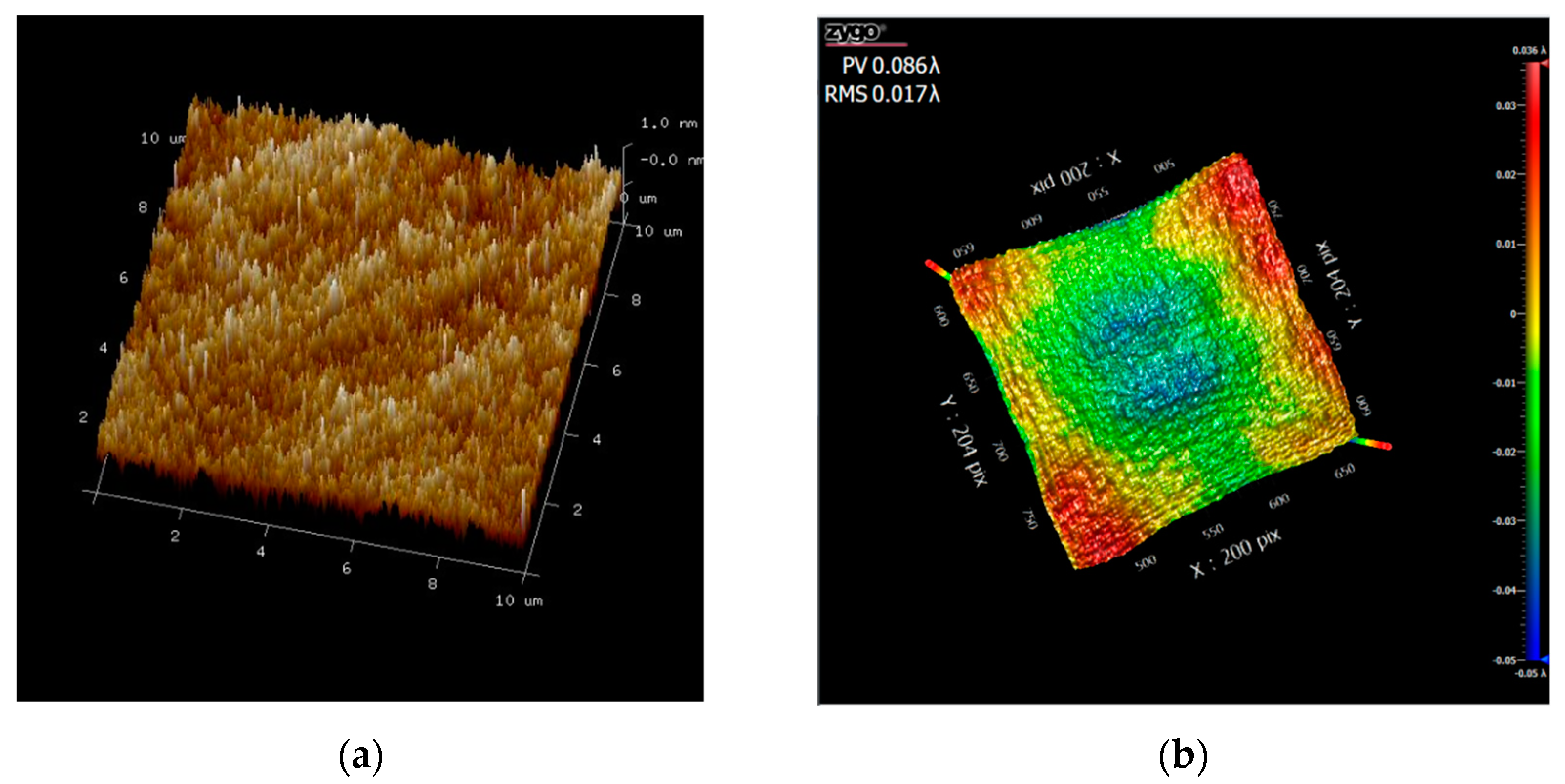
Figure 1, the ZGP samples (both the samples N1 and samples N2 elements) were polished to fit laser optic quality requirements (PV ≈ 55 nm, RMS ≈ 10 nm). For artificial polished samples, the roughness and the flatness was less than 0.233 nm and 0.683λ (at wavelength λ = 632.8 nm), respectively.
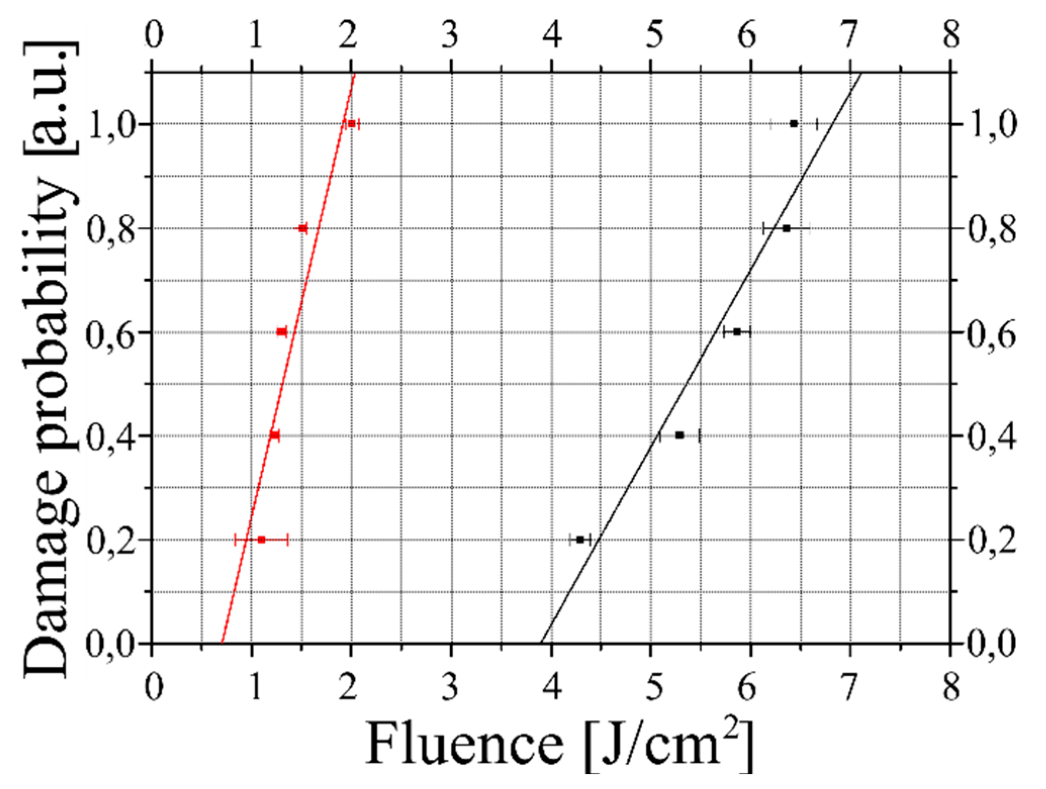
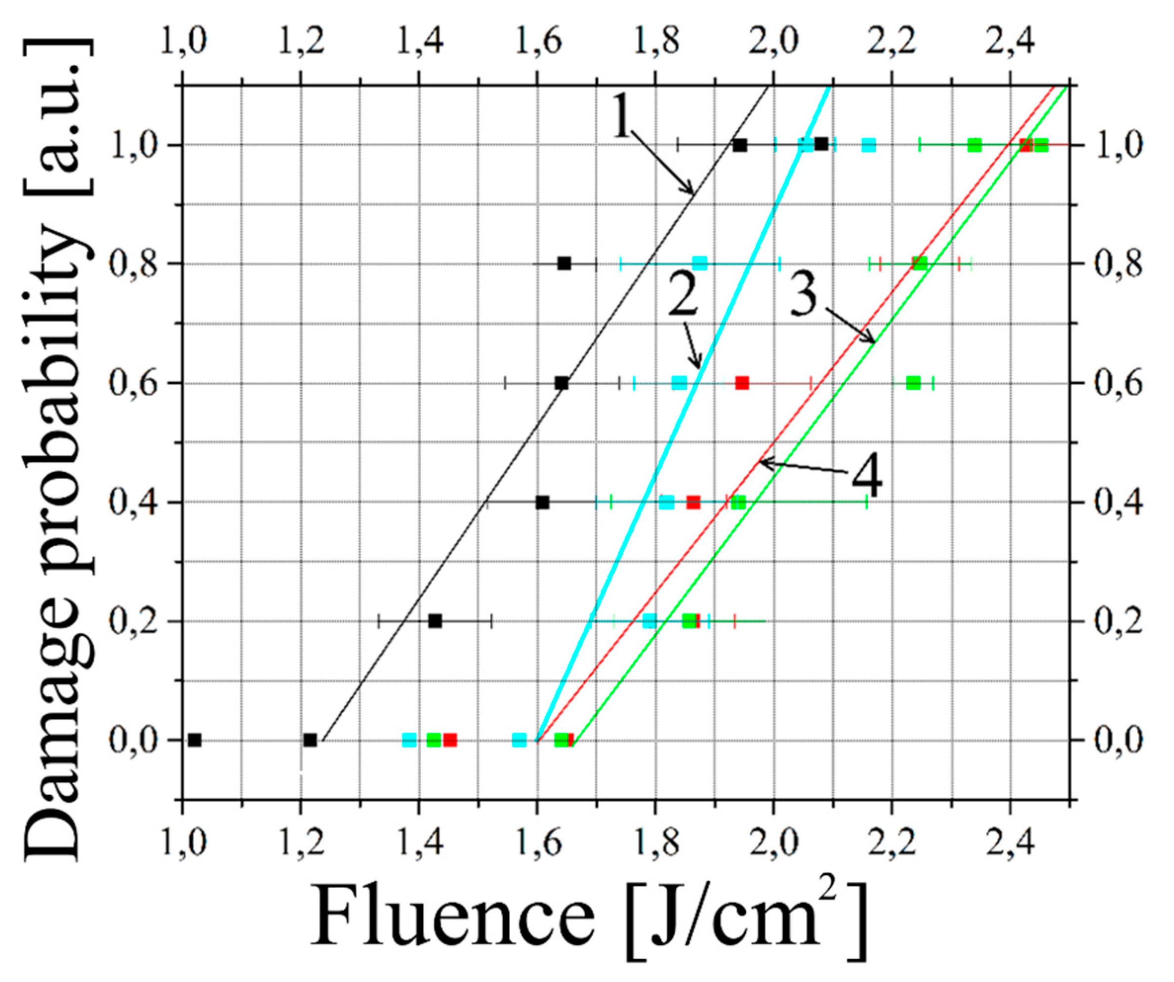
The probability of the optical damages of the samples N1 and samples N2 elements were compared at the same parameters of the experiments (PRR, the pulse width, the exposure duration) (
Figure 2).
The comparison of the experimental results and the calculated statistical parameters demonstrated 4-times higher LIDT (both the average fluence and the 0-probability LIDT fluence) for samples N2 in comparison with samples N1 (
Figure 2).
The critical values of the pulse fluence, peak and average power were measured to be much higher for the samples N2 elements compared to the samples N1 elements. It is well known that the ZGP LIDT depends on surface polishing [
14,
20].
The LIDs of the ZGP samples (manufactured in HIT or in LOC) were comparatively examined by the same R-on-1 test method and at the same test conditions: the testing laser wavelength was ~2.1 μm, the PRR was 10-12 kHz. The pulse width and the beam diameter of the Ho
3+:YAG laser were 18 ns or 35 ns, 180 μm or 350 μm (at the e
-2 level of the maximum intensity) for the HIT’s or LOC’s samples, respectively [
26,
30]. The measured ZGP LIDT for the pulse fluence was 3.45 J/cm
2 or 3.9 J/cm
2 for the LOC’s or HIT’s samples.
It was experimentally found that the change in the crystal growth technology resulted in the biggest increase in the LIDT. The growth conditions resulted in high lattice quality with a low occurrence of impurities. The improved growth technology leads also to reduce number of microdefects and a more uniform distribution of dislocations. This, in turn, resulted in higher optical homogeneity and higher LIDT of the material.
Various crystal impurities can affect the surface LIDT, both decreasing and increasing it. Recently it was reported, for example, the effect of the annealing atmosphere of chalcogenide crystals with the presence of Ar, Se and Zn on the mid-IR LIDT [
35]. For our presented studies influence impurity composition of LIDT, a ZGP single crystal (manufactured by LOC) was used, from which 8 samples were cut with (100) orientation and dimensions 5 × 5 × 2.45 mm
3. Mg, Se, Ca were thermally sputtered onto the pre-polished faces of the samples (the thickness of the sprayed film was 1 μm). After that, the ZGP samples with deposited films and two control samples without deposition were annealed in a sealed evacuated ampoule, into which a weighed amount of ZGP powder was added, at temperatures of 650°C for one set of samples and at 750°C for another similar set for 180 hours. After diffusion doping, the working surfaces of the test samples were re-polished. The LID of the obtained ZGP samples was tested by the following parameters of the Ho
3+:YAG laser: the pulse width was 35 ns, the PRR was 10 kHz, the laser beam diameter at the input surface of the studied samples was 350 ± 10 μm, similar as in the above-described experiments.
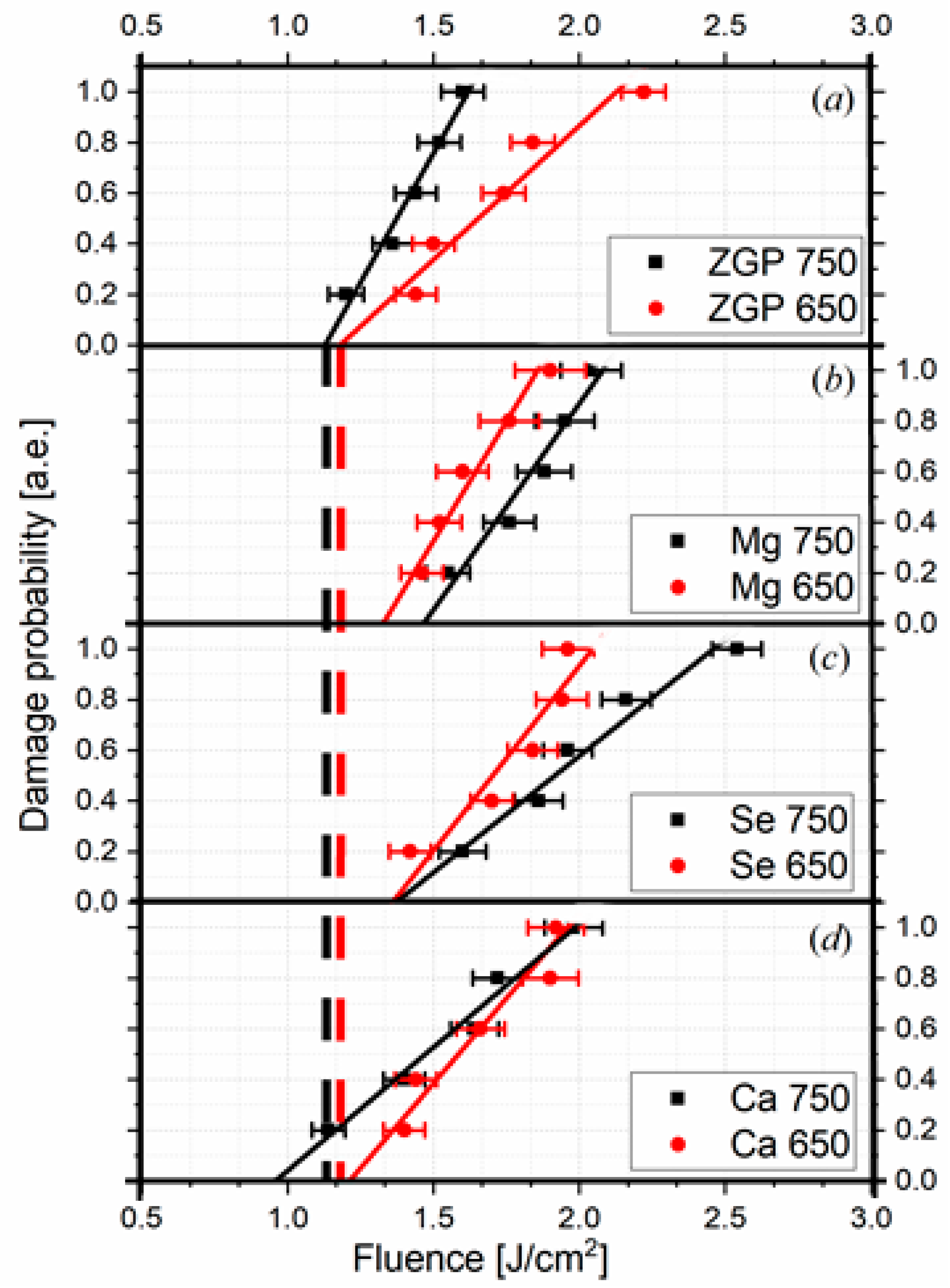
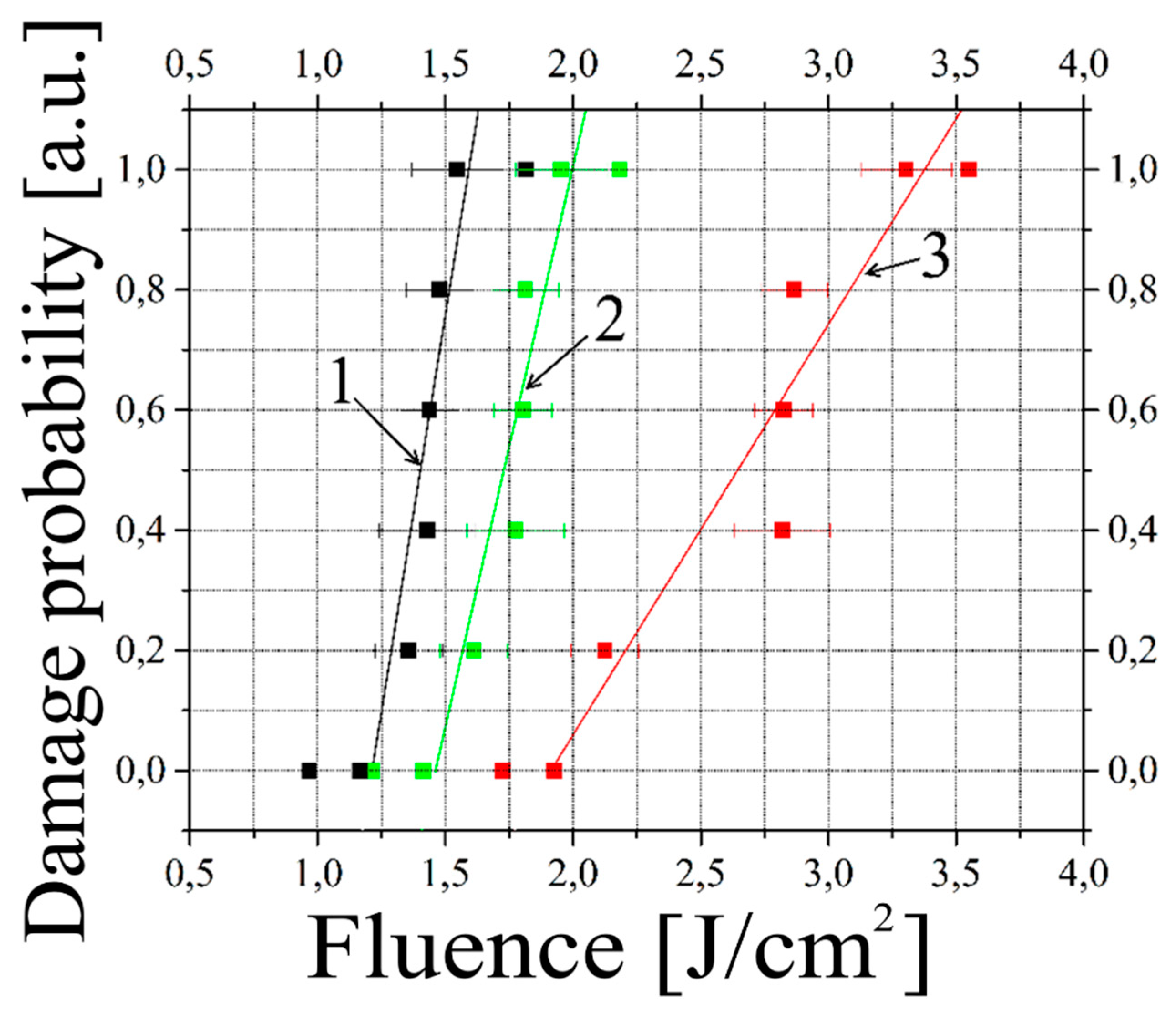
The results of measuring the LIDT of ZGP samples annealed at temperatures of 650 ⁰C and 750 ⁰C without doping and with doping Mg, Se and Ca using the R-on-1 method are shown in
Figure 3.
In the undoped samples (
Figure 3a), there are no significant changes in the LIDT (the detected changes were within the measurement error) depending on the annealing temperature, which is in good agreement with the results of [
17]. At the same time, in samples doped with Mg or Se by diffusion, after annealing at a temperature of 650°C, the LIDT increases by 15% and 17%, respectively. When annealing at a temperature of 750°C, the LIDT of samples doped with Mg and Se increased by 31% and 21%, respectively. An inverse dependence was observed for the sample doped with Ca. When annealing at a temperature of 650°C, the LIDT changes weren’t found, and when annealing at a temperature of 750°C, the damage threshold decreased by 14%. The presented results indicate a qualitative tendency for the LIDT to decrease or increase depending on the concentration of the doped material. It should be noted that for doped samples with Mg and Se, there was a tendency for LIDT to increase with increasing dopant concentration (since samples annealed at 750°C have a higher optical damage threshold than samples annealed at 650°C). An inverse dependence was observed for the samples doped with Ca by diffusion. The best results were the results of the single crystal ZGP doped with Mg at a temperature of 750°C.
From the results of measuring LIDT and electrical conductivity (
Table 2), a qualitative dependence can be seen. Doping with chemical elements causing a decrease in the electrical conductivity of the samples (σ) leads to an increase in LIDT, and vice versa, doping with chemical elements causing an increase in the electrical conductivity of the samples leads to a decrease in LIDT. For example, when ZGP is doped with calcium, σ increases by about an order of magnitude, while when ZGP is doped with Mg and Se, on the contrary, σ decreases by about an order of magnitude.
From the presented data in
Table 1, the diffusion doping with various chemical elements leads to increase or decrease in the LIDT.
LID in semiconductor materials at nanosecond pulse width can be a consequence of direct thermal effects or the electric-field-induced processes associated with the generation of electron-hole plasma [
36]. A local increase in temperature near small crystalline defects and inclusions under the pulsed radiation can initiate the LID. Indeed, point defects in a crystal lattice can enhance, for example, additional electronic sublevels, which facilitate multiphoton absorption at 2.09 μm and a sharp increase in temperature. The dislocation regions located inside the ZGP, especially near the surface of the sample, accumulate a number of point defects and inclusions, which provide an increase in temperature to a critical value. On the other hand, the local electric field at the dislocation point is stronger than in a homogeneous lattice, which lead to lower damage threshold enhanced by the electric field [
30]. Thus, it becomes obvious that the decrease in the conductivity of ZGP doped with Mg and Se should contribute to an increase of the LIDT.
4. Effect of external factors on LIDT ZGP
The effects of laser exposure duration and laser beam diameter on the LIDT of a ZGP crystal at room temperature as well as the effect of crystal temperature on LIDT were studied [
17]. The Ho
3+:YAG laser radiation at 2091 nm with 12 kHz PRR, 18 ns pulse width were used.
It was shown that with an increase in exposure duration from 2 to 30 s, the LIDT decreases by 1.2 times: from 1.57 to 1.28 J/cm
2 (
Figure 5).
Measurements at room temperature showed that with a decrease in the diameter of the test laser beam, LIDT increases: when the diameter of the beam is reduced by 2.9 times from 580 to 200 μm (at the level of e
-2), W
0d increased by 1.4 times, from 1.32 to 1.91 J/cm
2 (
Figure 6).
The increase in LIDT with a decrease in the diameter of the laser beam and the decrease in LIDT with an increase in exposure time can be explained by the thermal effects when the crystal is exposed to radiation at 2091 nm.
To study the temperature dependence of LIDT, in [
17] ZGP samples were placed in a sealed cuvette filled with dry nitrogen at normal pressure. Using a calorimetric cup filled with liquid nitrogen and having a thermal contact with the cuvette, the sample was cooled to a temperature of -106 °C (the sample temperature was controlled by an electronic thermometer). The windows of the cuvette were made of crystalline sapphire without AR coatings with a transmission coefficient (at 2091 nm) ≈ 85 %. The incident laser beam was focused onto the front face of the ZGP into a spot with a diameter of d ≈ 100 μm and into a spot with a diameter of d ≈ 270 μm.
At room temperature and a laser beam diameter of 270 μm, the threshold breakdown values for the ZGP sample were W
0d = 2.3 J/cm
2 and W
D = (3.4 ± 0.4) J/cm
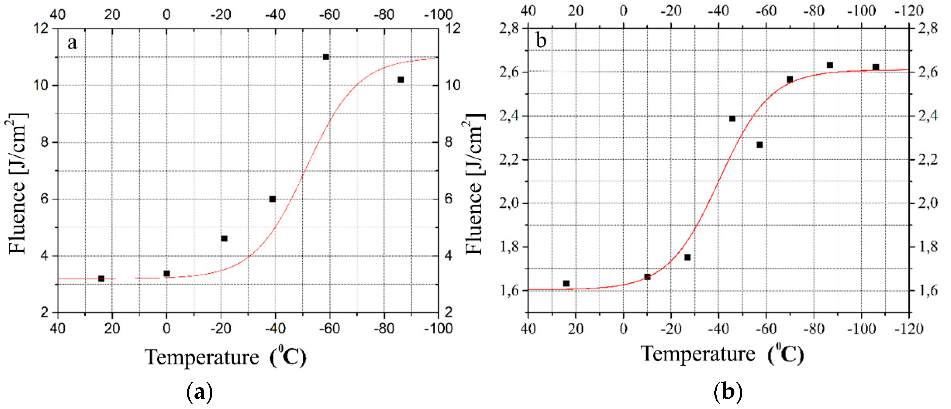
2. The measurement results demonstrated a significant increase in LIDT, especially noticeable when the temperature was reduced from 20 °C to -60 °C (
Figure 7a). In the temperature range from +24 to -86 °C, an increase in the LIDT value with a laser beam diameter of 100 μm was observed by more than 3 times (from 3.2 to 10.2 J/cm
2), however, at temperatures below -60 °C, the increase in LIDT stopped.
Measurements of the dependence of LIDT on the crystal temperature were also performed with a laser beam diameter of 270 μm. The measurement results demonstrated a similar dependence of LIDT on the crystal temperature (
Figure 7b). In the temperature range from +24 to -106 °C, an increase in the LIDT value of more than 1.5 times (from 1.6 to 2.6 J/cm
2) was observed, and the increase in LIDT also stopped at temperatures below -60 °C.
It is known that ZGP is a high-ohm semiconductor with stable hole conductivity, the magnitude of which is difficult to change [
37]. The typical temperature dependence of the concentration of free charge carriers in ZGP is described by an exponential curve with an activation energy of deep impurity centers of 0.3÷0.6 eV. However, the obtained temperature dependence of LIDT has a sigmoidal character and therefore cannot be explained by absorption on free carriers (holes), arising by ionization of individual point defects, as well as defects associated with edge dislocations.
The obtained temperature dependence of LIDT was explained by the temperature dependence of the phonon occupation numbers, which participate together with optical quanta in indirect transitions of nonlinear absorption: valence band - impurity level [
38]. In support of this assumption, it can be noted that with a decrease in the temperature of the crystal, the phonon occupation numbers increase, leading to a decrease in the probability of their participation in indirect transitions of electrons from the valence band to impurity levels [
39].
5. Dynamic processes in the ZGP pre-damage region
Modern technologies allow using a CCD camera to register the interference pattern of the reference and object waves. This process of recording holograms on a CCD camera and subsequent numerical recovery of an image from them is called digital holography.
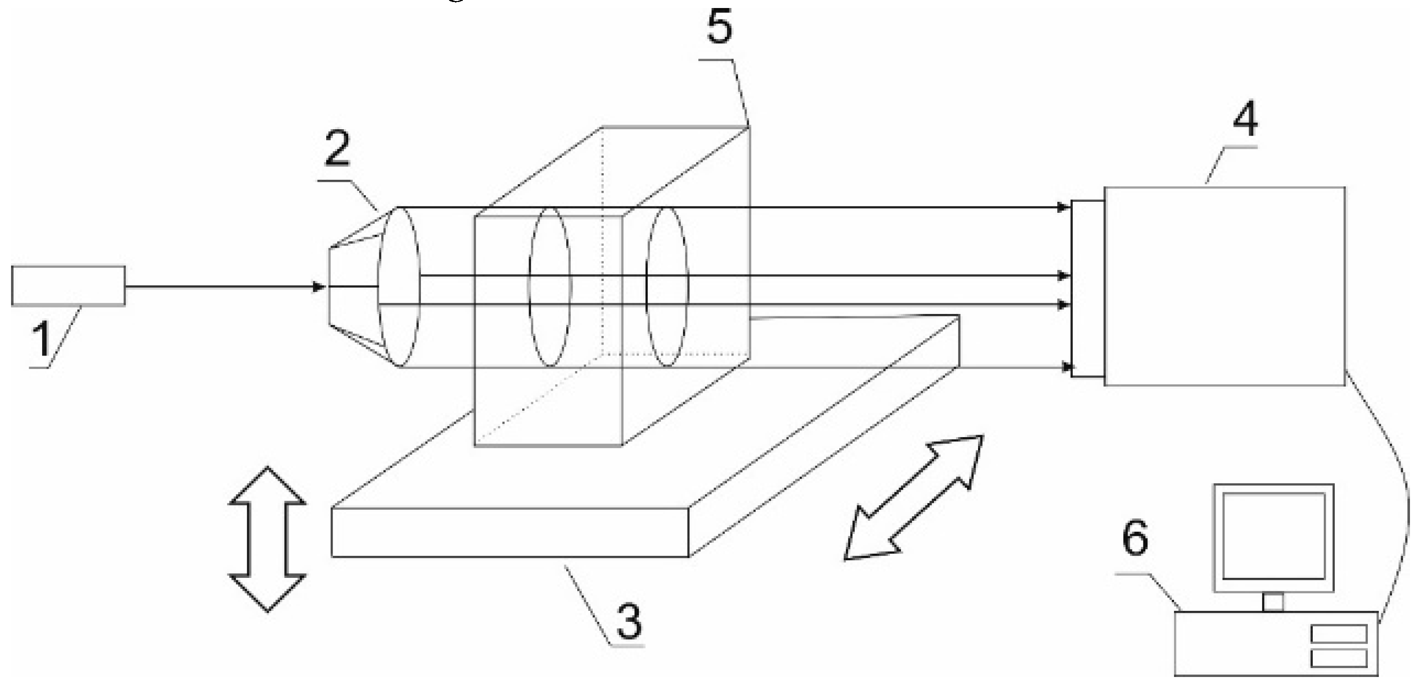
Figure 7 shows the axial scheme of recording Gabor digital holograms. Light from a laser source (1) passes through a collimator (2), forming a beam of the required cross section, then passes through the sample under study.
As a result, an interference pattern of the reference (part of the radiation that passed by the inclusions) and object (part of the radiation scattered by the inclusions) waves is formed. The camera registers this interference pattern and transfers it to the computer memory. Subsequent mathematical processing by special computational algorithms [
40] allows to restore the spatial distribution in the investigated volume, namely three-dimensional coordinates, sizes, shapes, and location of each area of interest. Image restoration is numerical, with the image of the investigated volume being formed during processing layer by layer.
Since the Gabor scheme allows for reduced requirements for the spatial and temporal coherence of the light source [
41], a semiconductor laser diode with a wavelength of 1.064 μm (position 1 in
Figure 8) with an output power of 100 mWwas used in [
15]. A CCD camera with a matrix of 1600 × 1200 pixels, a pixel size of 7.4 μm × 7.4 μm, and physical dimensions of the matrix of 2/3” was used as the recording camera (position 4 in
Figure 8). The long-wavelength boundary of the CCD camera's photosensitivity is limited to a wavelength of 1.1 μm. The spectral transparency range of the ZnGeP
2 compound, calculated for short wavelengths based on the bandgap width and for the long-wavelength edge based on the maximum three-phonon absorption, includes the region of 0.64 – 9.0 μm, but the actual working spectral range at a coefficient of absorption not exceeding a value of 1 cm
-1 is determined by wavelengths in the range of 0.9 ÷ 8.3 μm. Thus, for studies of ZnGeP
2 using digital holography on "transparency", sources that generate radiation in the spectral region near 1.06 μm and CCD matrices of the visible range can be used. These issues are discussed in detail in [
42].
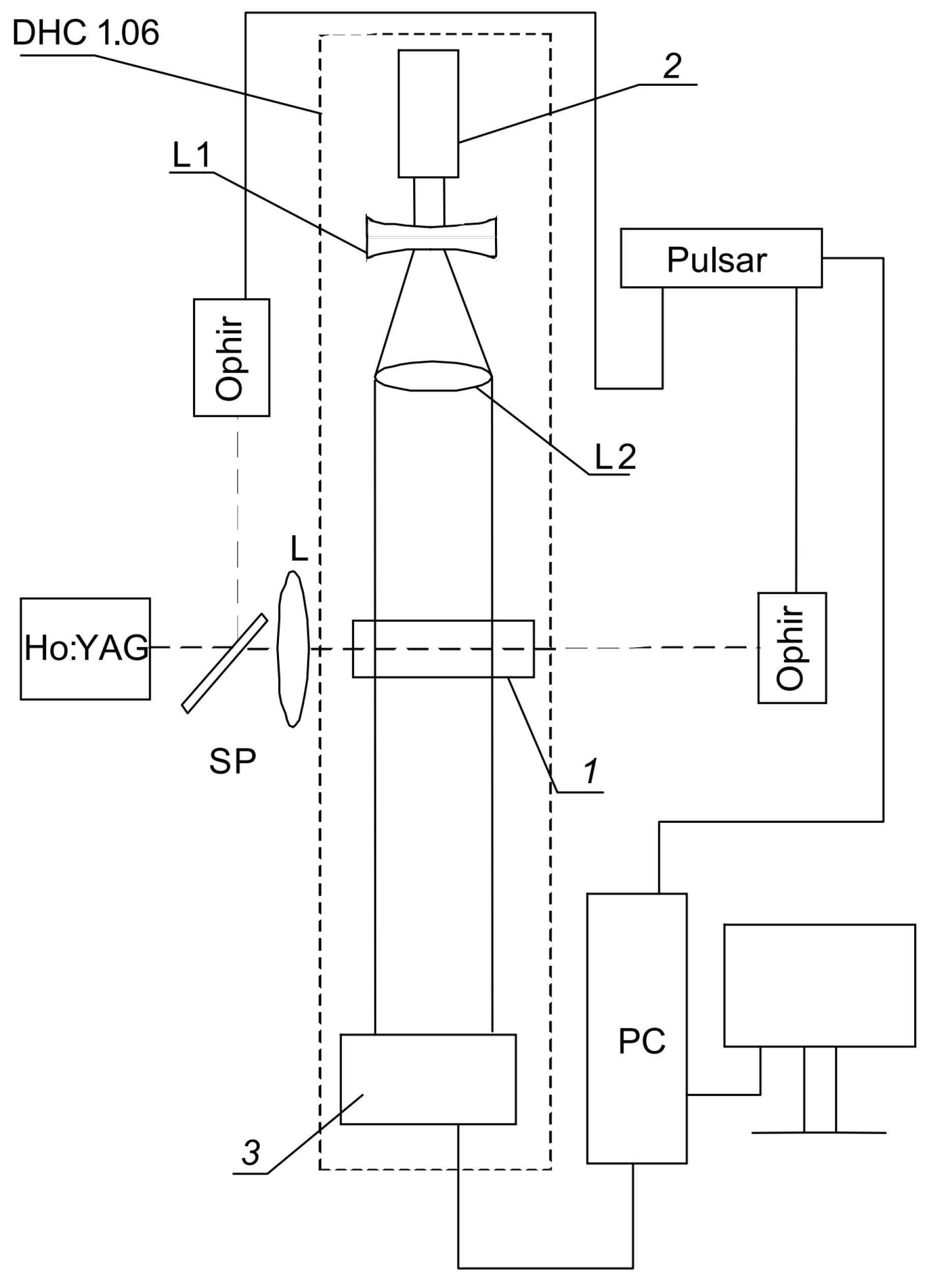
It is clear that the investigated area is limited by the camera aperture of ~ 11 mm. The holographic camera was used to study the ZGP optical damage, designed for the creation of parametric converters of radiation tunable in the range of 3-8 μm, pumped by lasers emitting in the wavelength range of about 2 μm. The study of LID was carried out using a scheme of the digital hologram recording (
Figure 8). Pulsed radiation from a Ho
3+:YAG laser with a PRR of ~ 10 kHz, pulse width of ~ 25 ns, and average power, varied from 500 mW to 9 W, was focused by a short-focus lens L, onto the input face of a ZGP single crystal (manufactured by LOC). The use of a short-focus lens excluded self-focusing of radiation in the volume of the investigated crystal. The exposure duration was ~30 s. Further, if optical damage wasn’t observed, the laser radiation power was increased, and the irradiation process was repeated. The beam diameter at the front face of the single crystal was ~ 200 μm at the 1/e
2 level. The side faces of the crystal were polished. The crystal was placed in a digital holographic camera DGK 1.06, using which holograms of the internal volume of the single crystal (in the direction perpendicular to the direction of the incident radiation) were recorded with a frame rate of ~ 7 Hz.
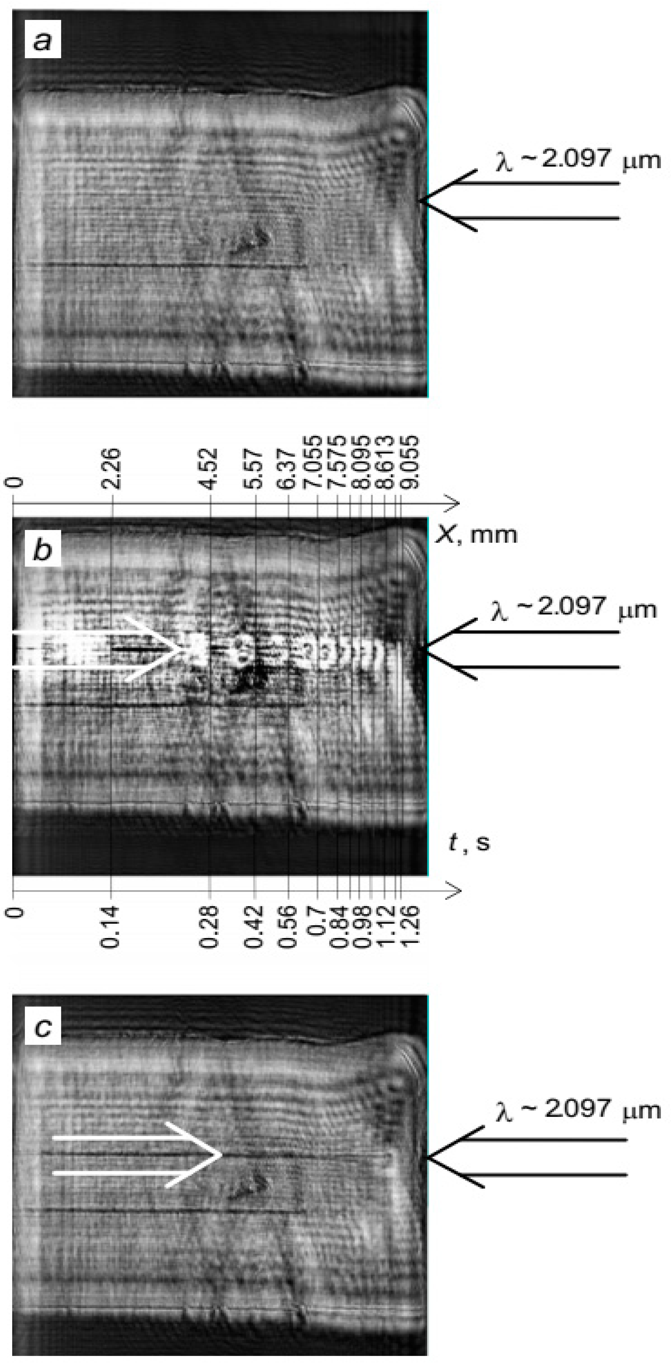
Figure 10 shows the reconstructed images obtained in the study of optical damage on the setup shown in
Figure 9.
Figure 10a shows the reconstructed image of the plane of the best installation of the area of the single crystal where the breakdown develops, before the formation of the damage track and the formation of the glowing area, the red arrow shows the direction of the radiation incidence.
Figure 10b is a splicing of frames of the reconstructed image of the plane of the best installation, on which the process of development of optical damage and the spread of the glowing area in the single crystal is recorded with reference to the length of the crystal and time, the red arrow shows the direction of the radiation incidence, the yellow arrow shows the direction of movement of the area in which the optical damage is formed.
Figure 10c is the reconstructed image of the plane of the best installation of the area of the single crystal with a characteristic damage track above LIDT.
The impact of the Ho
3+:YAG laser pulses on the ZGP crystal caused the appearance of a luminous spot with a diameter of 0.7-1 mm on the output optical surface, and its subsequent movement in the crystal towards the input optical surface, i.e. in the direction opposite to the propagation of the Ho
3+:YAG laser radiation (
Figure 10b). The resulting luminous spot can be associated with luminescence arising from the recombination of non-equilibrium carriers through the levels of point defects [
15]. The movement of the luminescent "cloud" is accompanied by the formation of an optical damage channel (track) with a diameter of 70-75 µm. The dynamics of the development of optical damage at an average laser fluence of 0.3 J/cm
2 is shown in
Figure 10b, which was obtained by splicing frames reconstructed from a series of holograms obtained with an interval of ~143 ms. The frames are separated from each other by black lines, each frame corresponds to the path traveled by the luminous spot that is fixed when the damage track is formed inside the crystal.
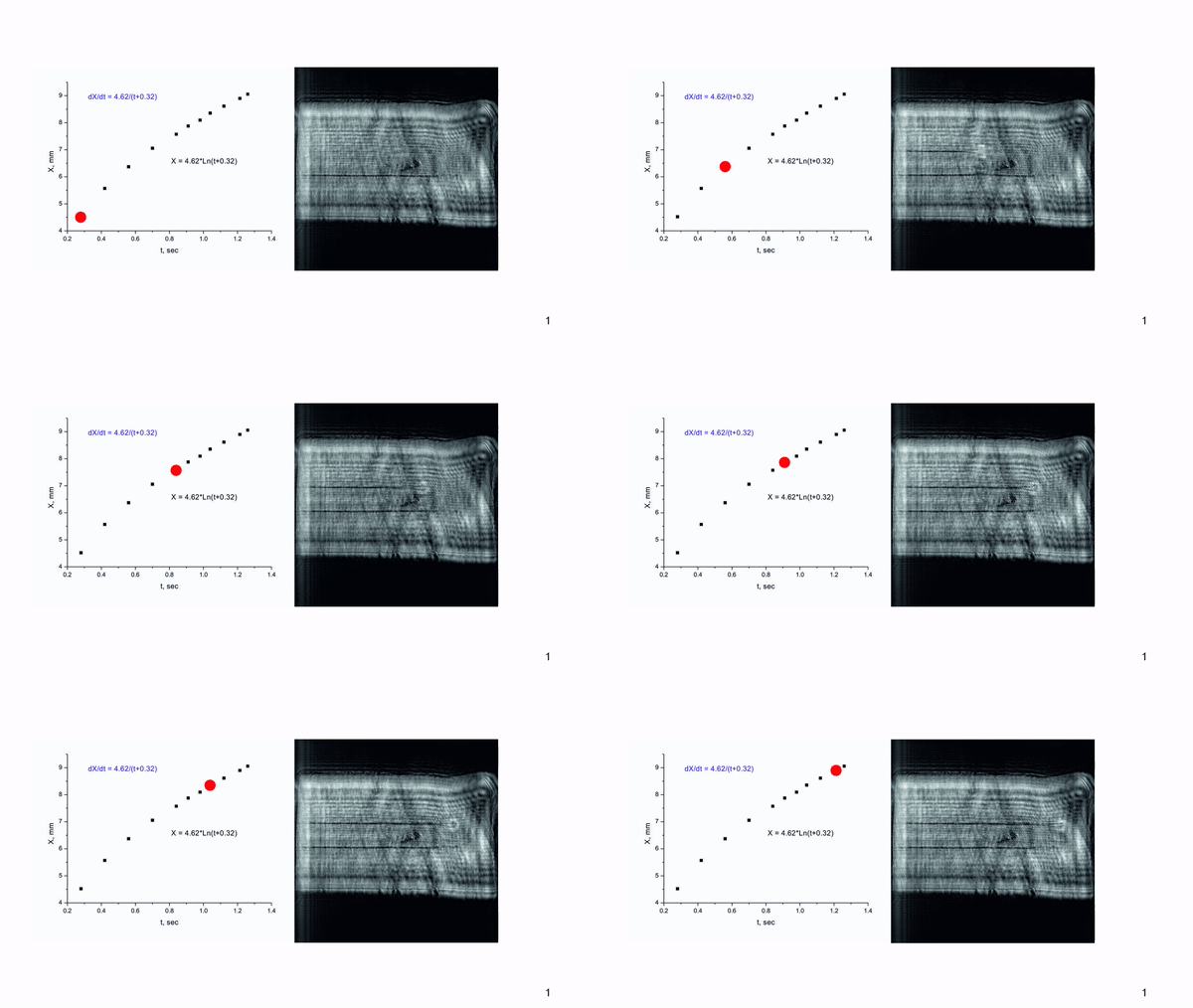
The position of the luminous spot relative to the exit crystal face, X, was determined at the time,
t , relative to the LID start (
Figure 11).
The full duration of the optical damage formation in a 10 mm ZGP crystal was determined as ~1.3 seconds. The instantaneous speed of movement of the luminous spot - V (mm/s) =dX/dt - in the initial period, as it turned out, was significantly higher than the speed of its advancement in the second half of the crystal. So, if the first 4.5 mm were damaged with a speed of Vin= 4.52/0.28 ≈ 16 mm/s, then at the final stage of the damage, the speed of track formation was Vfin= (9.055-8.095)/0.14 ≈ 3 mm/s. The damage stops at the destruction of the entrance face of the crystal,.
Using the available experimental data and the ORIGIN LAB mathematical software, a logarithmic dependence of the track length on the time of exposure was obtained (see
Figure 11). The dependence of the speed of propagation of the luminous spot in a ZGP crystal at the beam fluence of 0.3 J/cm
2 obtained by the least squares method is a smooth monotonic function of the current time:
where
t is the time in seconds relative to the LID initial moment (when the glowing spot appeared).
According to the given approximation, the speeds of the spot propagation (the damage track formation) were determined as Vin = 14.4 mm/s at the initial stage, and Vfin = 3.5 mm/s at the final stage of the LID. The slowing down of the track formation process isn’t consistent with the impact ionization model with a power law dependence of the avalanche generation of electron-hole plasma. At the same time, positive feedback between the temperature increase and the ZGP absorption coefficient increase can be an alternative to impact ionization and can provide a high concentration of non-equilibrium carriers due to a sharp temperature jump during the absorption of pumping radiation in the crystal volume. Then, the time delay of the beginning of track formation can be attributed to the time spent on heating the crystal volume to high temperatures by laser radiation.
The generation of carriers by increasing temperature does not create non-equilibrium carriers capable of recombination accompanied by luminescence. Therefore, in order to explain the appearance of a luminous area in the crystal excited by an intense laser beam, it was necessary to take into account dimensional factors, namely: the ratio of the diameters of the laser beam (200 μm) and the luminescent "cloud", the brightest glow of which is recorded at a distance of 250-400 μm (
Figure 10b) from the forming "dark" LID track.
The change in the crystal structure under the laser irradiation indicates an increase in the instantaneous effective temperature to values that exceed the melting point of the ZGP compound - 1025⁰ C [
15,
42]. A lower-temperature phase transition ZnGeP
2(sph)→ZnGeP
2 (halc) near 950⁰ C can be excluded from consideration, since it is observed only at low temperatures and is associated with the ordering of atoms in the caution sub lattice.
A sharp increase in the temperature of the crystal and its local melting led to subsequent solidification of the melt, forming a LID track along the laser beam, and diffusion of free carriers from the heated area of the crystal in the direction perpendicular to the laser beam. The transverse temperature gradient perpendicular to the direction of propagation of laser radiation causes free carriers to diffuse from the high-temperature generation zone (in which they are in equilibrium and cannot be manifested in luminescence) to the unheated regions of the crystal, in which they become non-equilibrium and recombine, at least partially, at the luminescence transitions (levels of point defects), creating a toroidal distribution of the intensity of luminescence.
In order to explain the decrease in the speed of formation of the damage tracks from the coordinate (from the time), in [
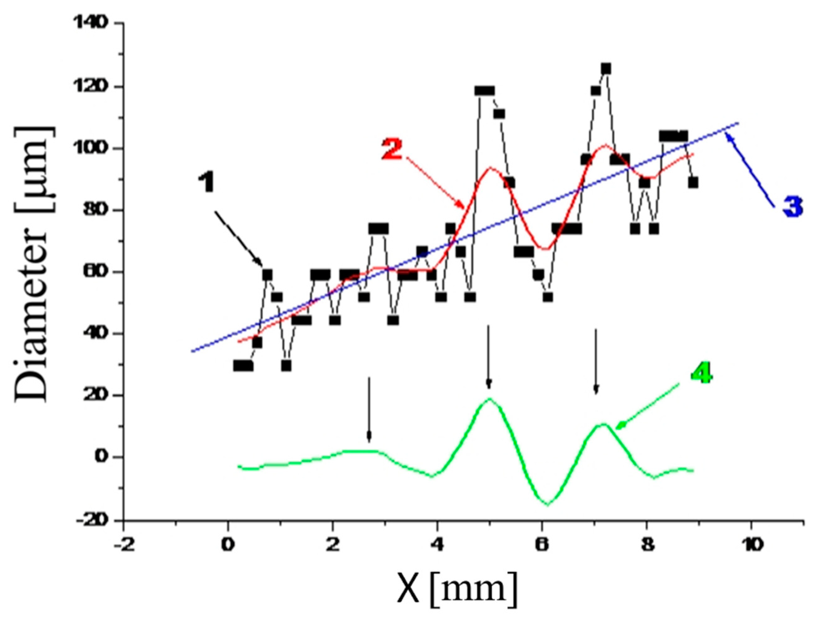
15] it was assumed that it is related to the conical form of the track, i.e. with the volume of the material heated by the laser beam. As it turned out, (see
Figure 12), indeed, the diameter of the track increases from ≈40 μm at the initial section of the track to ≈100 μm at the input aperture of the crystal. Accordingly, the cross-section changes by approximately 3-4 times, which is close to the ratio of the track formation speeds on the input and output surfaces of the crystal. But in addition to the pronounced tendency for the track diameter to increase with the coordinate, there were quasi-periodic variations in the diameter of the LID tracks with maxima at ≈3 mm, 5 mm, and 7 mm, which were compared with areas near the intersection points of the optical damage track with "dark" growth bands, i.e. in places with an increased absorption coefficient, relative to the average value.
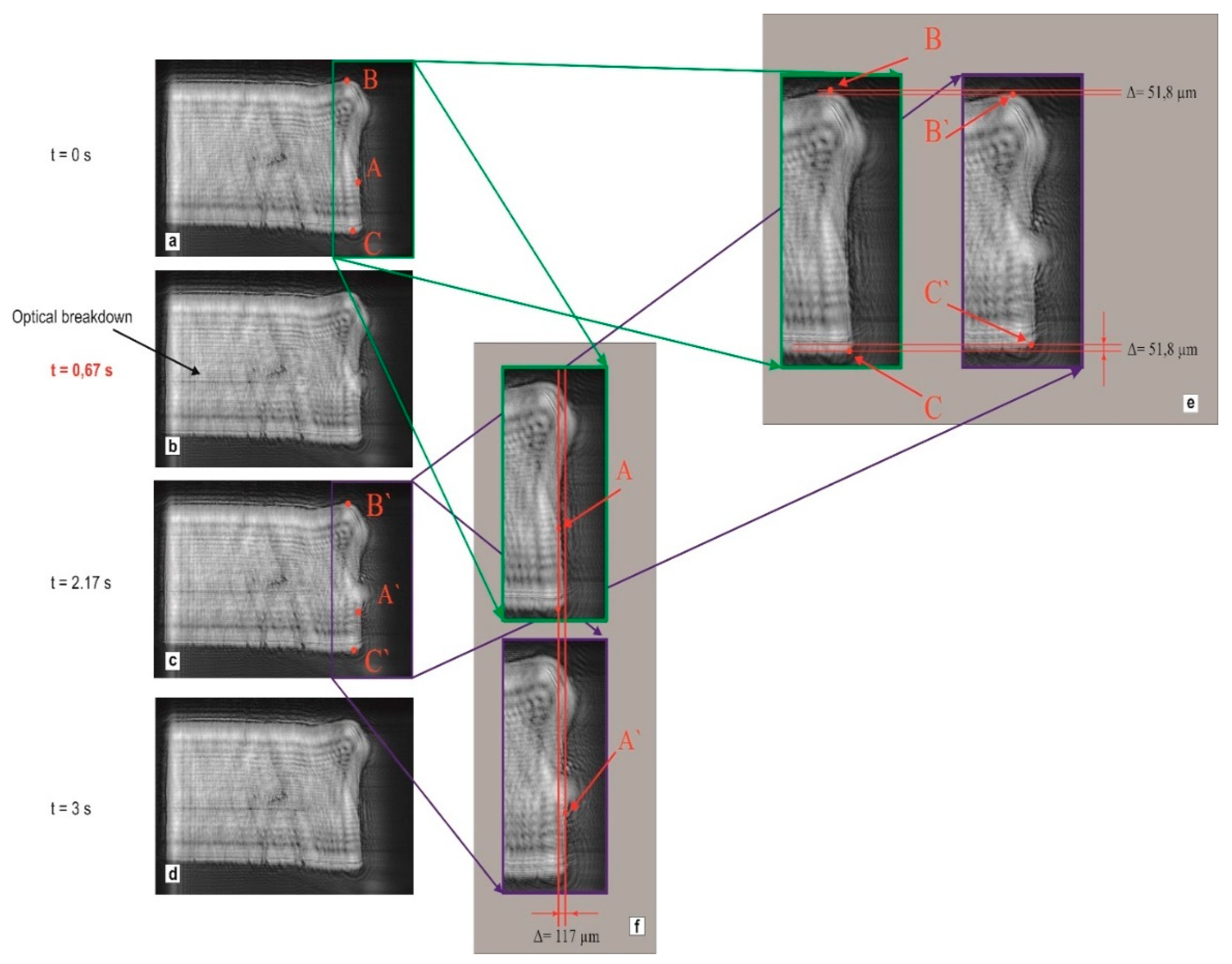
Figure 13 shows a LID in another point of the same crystal under the more powerful laser irradiation – with the fluence of 0.6 J/cm
2. In this case, the optical damage also occurred near the exit surface, but the track formation process proceeds significantly 2 times faster, which, in principle, agrees with the twofold increase in the beam fluence and the thermal origin of the LID. Processing of holographic data shows that the duration of the damage-track formation was ~0.67 s.
On the photographs in
Figure 13f,e, the reconstructed images of the crystal before laser exposure and at the moment when the glowing (luminescent) spot reaches the front surface of the crystal are shown. By comparing the geometric (dimensional) parameters of the images, it was found that at the final stage of optical damage, when the formation of the track is completed, the length of the crystal in the longitudinal direction at the point of exit of the track to the surface increases by ~ dL=117 μm (
Figure 13f), and in the transverse direction it decreases by ~ 103 μm (
Figure 13e).
A rough estimate of the temperature developing in the central part of the damage track can be made based on the relative longitudinal deformation of the crystal dL/L ≈ 0.0117 and coefficients of thermal expansion (
βav) of ZGP [
15,
43]. At temperature of > 573 K the coefficient of thermal expansion has the value
. The temperature required for an elongation of the crystal by 117 μm can be estimated by
. Therefore, according to the estimation, to change the length of the crystal by 117 μm, it will be necessary to increase its temperature to
. The obtained value of the temperature in the damage track is higher than the melting point of the compound by approximately ≈ 60 K and, in principle, agrees with the conclusion about the thermal origin of the LID track.
At the used levels of laser beam intensity, in contrast to the degradation of optical properties in the damaged region, the mechanical deformation of the crystal was elastic, and after the completion of the damage track formation process, a rapid lattice relaxation occurs along the entire length of the crystal.
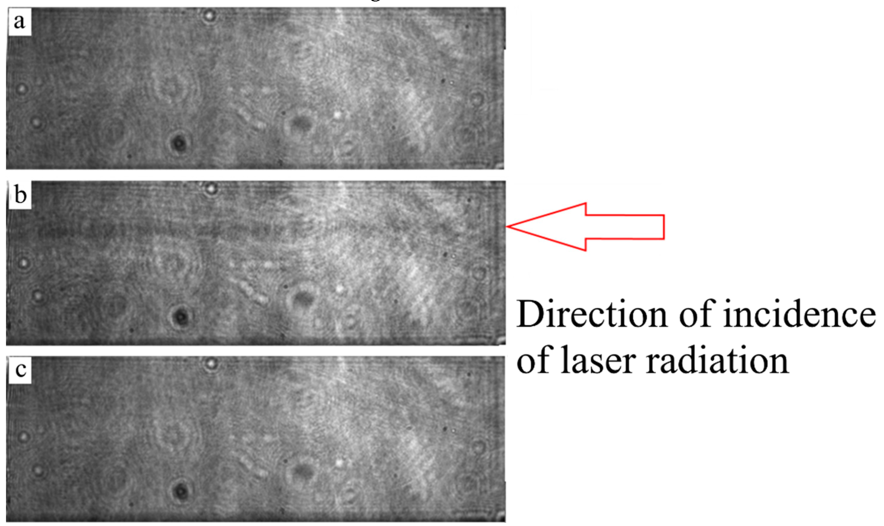
As a result of comparative studies of the crystal before, during, and after LID, it was established that the propagation channel of laser radiation darkens in the pre-damage region of the laser parameters. Visually, this effect manifested itself in the reconstructed images of the plane of the best setup in the form of darkening of the area of the crystal in which laser radiation was propagated (
Figure 14). This process is clearly demonstrated in
Figure 14b: a dark track is formed in the channel of propagation of an intense laser beam (for test radiation at a wavelength of 1064 nm). The darkening was reversible: when the density of the incident radiation decreased below a certain level or when laser exposure to the crystal was completely stopped, the area of darkening disappeared -
Figure 14c. The relaxation time of the area of darkening of the laser channel was less than 5 ms.
The darkening of the channel of propagation of a powerful laser beam in the pre-damage region can be explained by a local decrease in the band gap width of ZGP upon heating. Indeed, it is known that the band gap width of semiconductors decreases with increasing temperature [
17]. This leads to an increase of the absorption of the testing beam at 1064 nm.
Importantly, in most of the tests performed with ZGP elements of different lengths and manufactured with different technological growing and post-growing procedures (in more than 90 % of the total number of measurements), the LID began at the exit surface of the sample. The LIDT difference on the exit and entrance surfaces can be explained by the different intensity (and the fluence) of the laser beam at the surfaces. The last difference could be caused by two effects: thermal self-focusing (the thermal lens formation) in the ZGP crystal [
44], and a difference in the maximum electric field amplitude of the optical waves at the surfaces due to a phase difference of the waves reflected from the boundaries [
45]. The thermal self-focusing may be the impotent effect for the long samples or the ZGP-tandem OPOs [
46], when the focal length is comparable with the element length. The second effect of the interference between incident and reflected waves at the surfaces of a sample (depended on the boundary phase changes) appears to be more reasonable for the thin element with low absorption [
47]. Indeed, the ratio of the exit to entrance wave intesities
Iex and
Ient, respectvely, can be estimated (on the crystal boundaries without any AR coating and higher order reflections) by the following expression [
45]:
where
n is the refractive index,
α is the absorption coefficient,
L is the sample length. The estimation of the intensity ratio by Expression (2) for the ZGP crystal with the refractive index of ~ 3.15 (at 2.1 µm [
48]) gives 2.3×exp (-αL). This value is more than 1 for αL < 0.83. Therefore, the scenario with the LID initiation near the exit surface due to the higher intensity of the exit beam appears to be quite natural even for a long ZPG sample with the length
L = 3 cm and the absorption coefficient α < 0.28 cm
-1 (the used ZGP samples had the much lower absorption coefficient).
6. Effect of pre-damage phenomena on ZGP OPO operation
A transparent nonlinear ZGP crystal (produced by LOC) with linear dimensions of 20x6x6 mm
3 cuted at angles θ ≈ 54.5° and φ ≈ 0° was used to examine an effect of the pre-damage phenomena on ZGP OPO operation [
49]. The absorption of radiation at a wavelength of 2.097 μm of the sample was 0.029 cm
-1.
The scheme of the experimental setup is shown in
Figure 15. A periodically pulsed Ho
3+:YAG laser was used as a pump source for the OPO. Optical isolation between the OPO cavity and the Ho
3+:YAG laser cavity is provided by an optical isolator (OI).
Table 3 YAG laser used for the experiments had the following energy characteristics: maximum average power of radiation in pulsed mode was 15 W, PRR was 10 kHz, pulse width at half-height was 26 ns. The OPO cavity was formed by a plane mirror M1 with transmission of ~99% at the pump wavelength and reflection of ~99% at the generated wavelength. The plane mirror M2 had a transparent coating with transmission of ~99% at the pump wavelength with a beam-splitter coating with 50% reflection at the generation wavelength, which made it possible to implement single-pass pumping. The ZGP crystal with AR coatings applied to the working surfaces at wavelengths of λ = 2.097 μm and λ = 3.5 -5 μm was placed in the cavity formed by mirrors M1 and M2. The side faces of the ZGP element were also polished. Through the side polished surfaces of the ZGP element, a hologram of the internal volume of the crystal (in the direction perpendicular to the direction of the incident radiation) was recorded using a digital holographic camera.
The results obtained from measuring the energy characteristics of the ZGP OPO with Ho
3+:YAG laser pumping are presented in
Figure 16,
Figure 17 and
Figure 18.
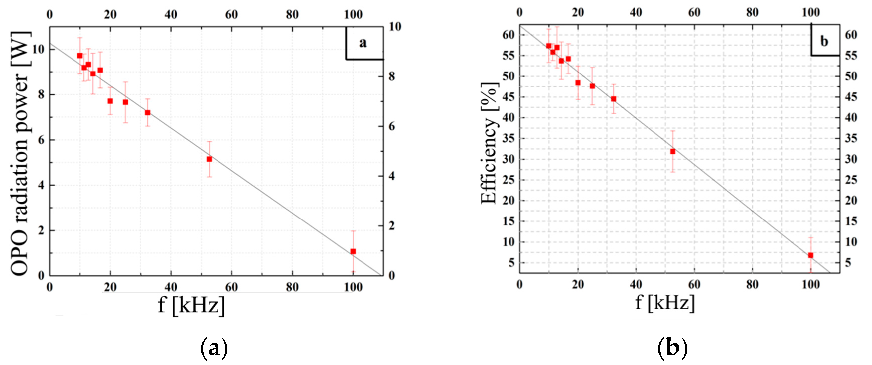
Figure 16 shows the dependence of the average power of radiation generated in the OPO and the generation efficiency on the PRR pumping.
During the measurements, the average pump power at 2.097 μm remained constant at 16.3 W, while the PRR was varied from 10 to 100 kHz. It is worth noting that stable generation in the Ho
3+:YAG laser was observed up to 50 kHz PRR, at a PRR of 100 kHz, the laser operation was unstable. The maximum value of the OPO efficiency achieved in the experiment was 57.35% (
Figure 16b). The maximum value of the OPO average power was 9.72 W at the PRR of 10 kHz (
Figure 16a).
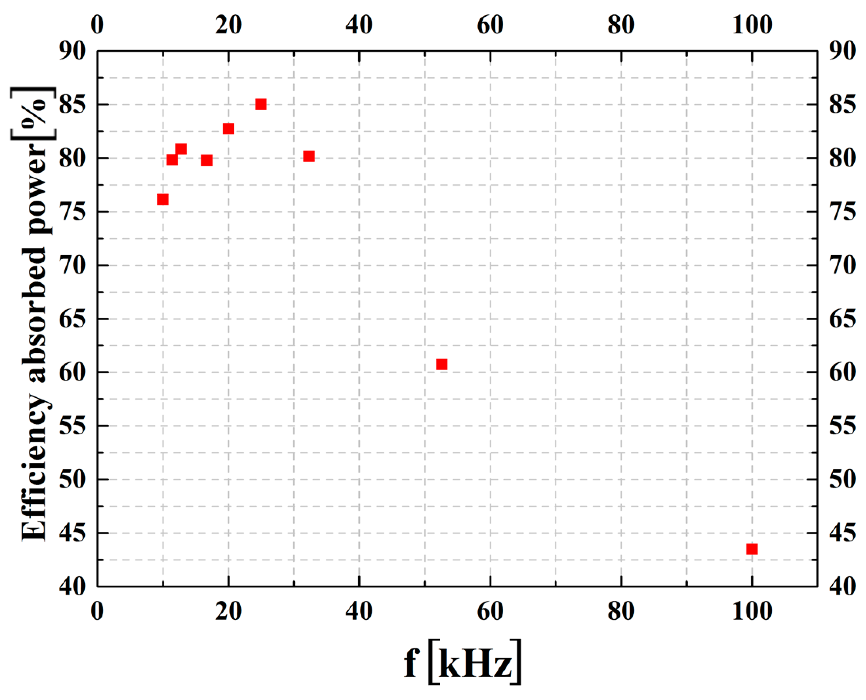
Using the available experimental data and the ORIGIN LAB mathematical software, the dependence of the efficiency of the pump power absorbed in the crystal (without taking into account the part of the pump power that escaped from the cavity) on the pumping PRR was obtained. The maximum value of the efficiency of the absorbed power was ~ 85% (
Figure 17).
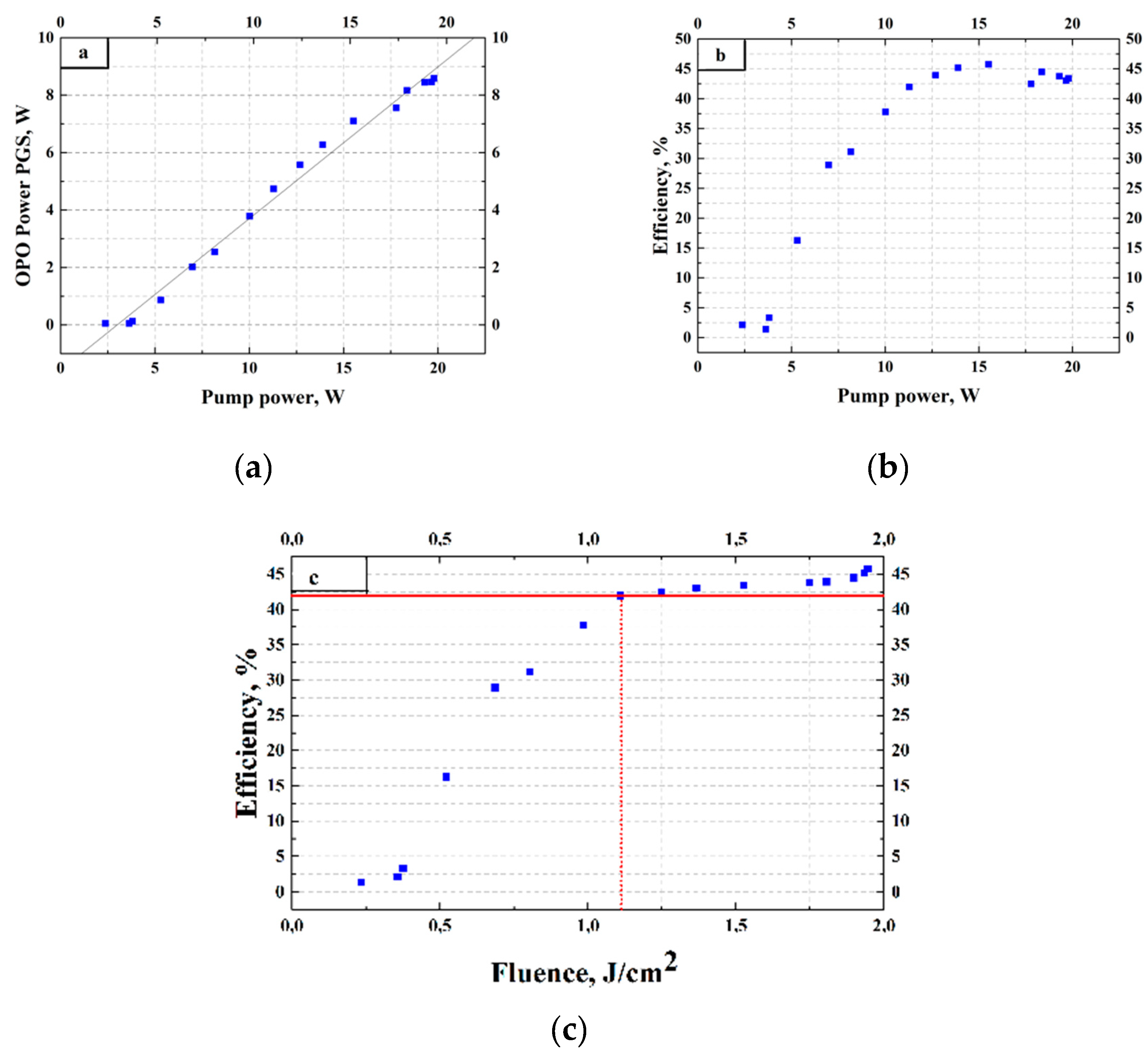
Further studies were conducted of the energy characteristics depending on the pump power at a PRR of 10 kHz. The maximum value of the OPO output power obtained in the experiment was 8.46 W (
Figure 18).
The maximum efficiency is ~45.74%. From
Figure 18c, it is clear that when the pump power reaches ~11 W and the energy density reaches ~1.2 J/cm
2, the efficiency stops growing and reaches a saturation point.
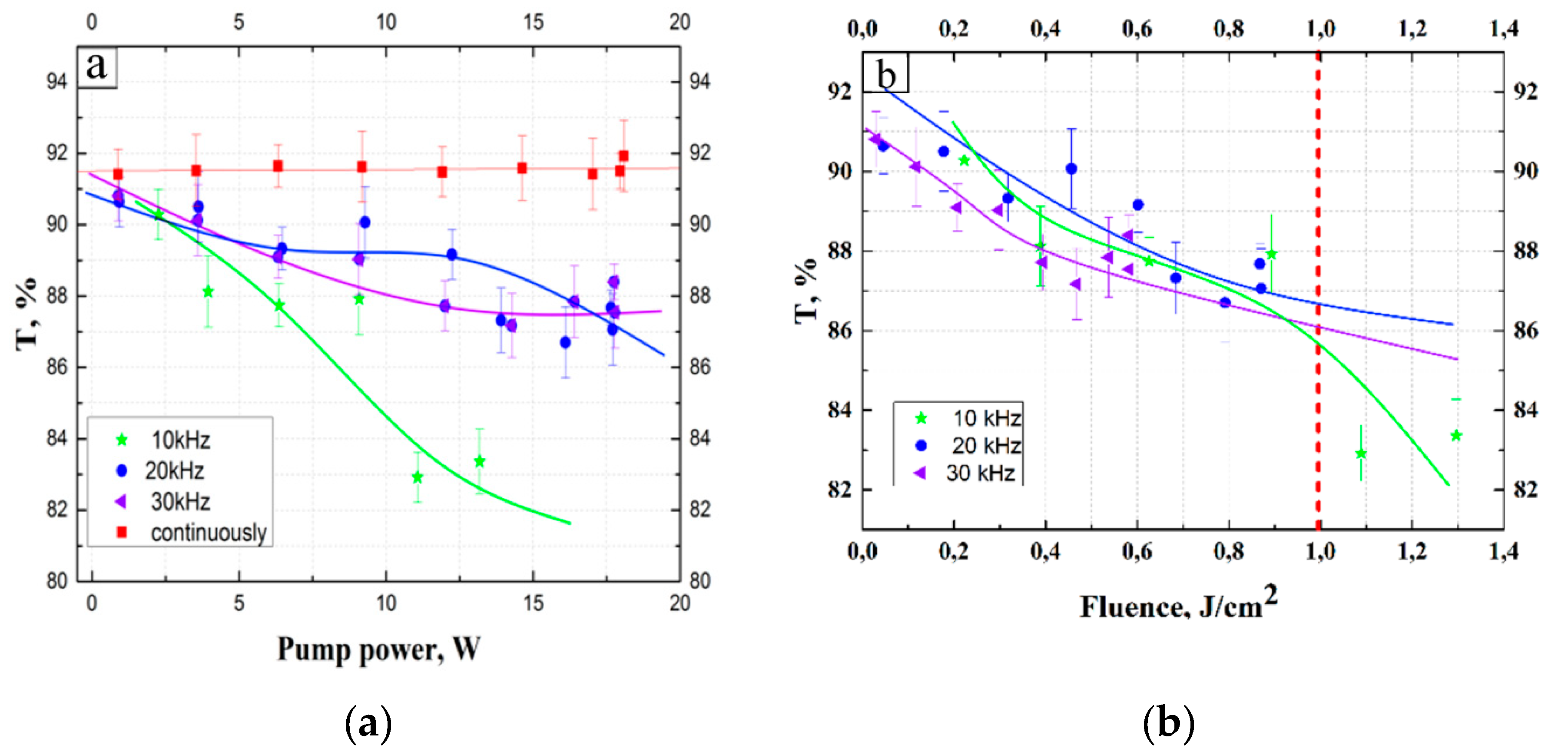
Studies were conducted on the dependence of the transmission of the nonlinear crystal on the power of the test radiation and on the energy density of the radiation falling on the crystal. The results obtained (
Figure 19) were presented in the form of dependencies of the transmission on the pump power and the transmission on the energy density of the radiation falling on the crystal, the PRR was varied from 10 kHz to 30 kHz with a step of 10 kHz.
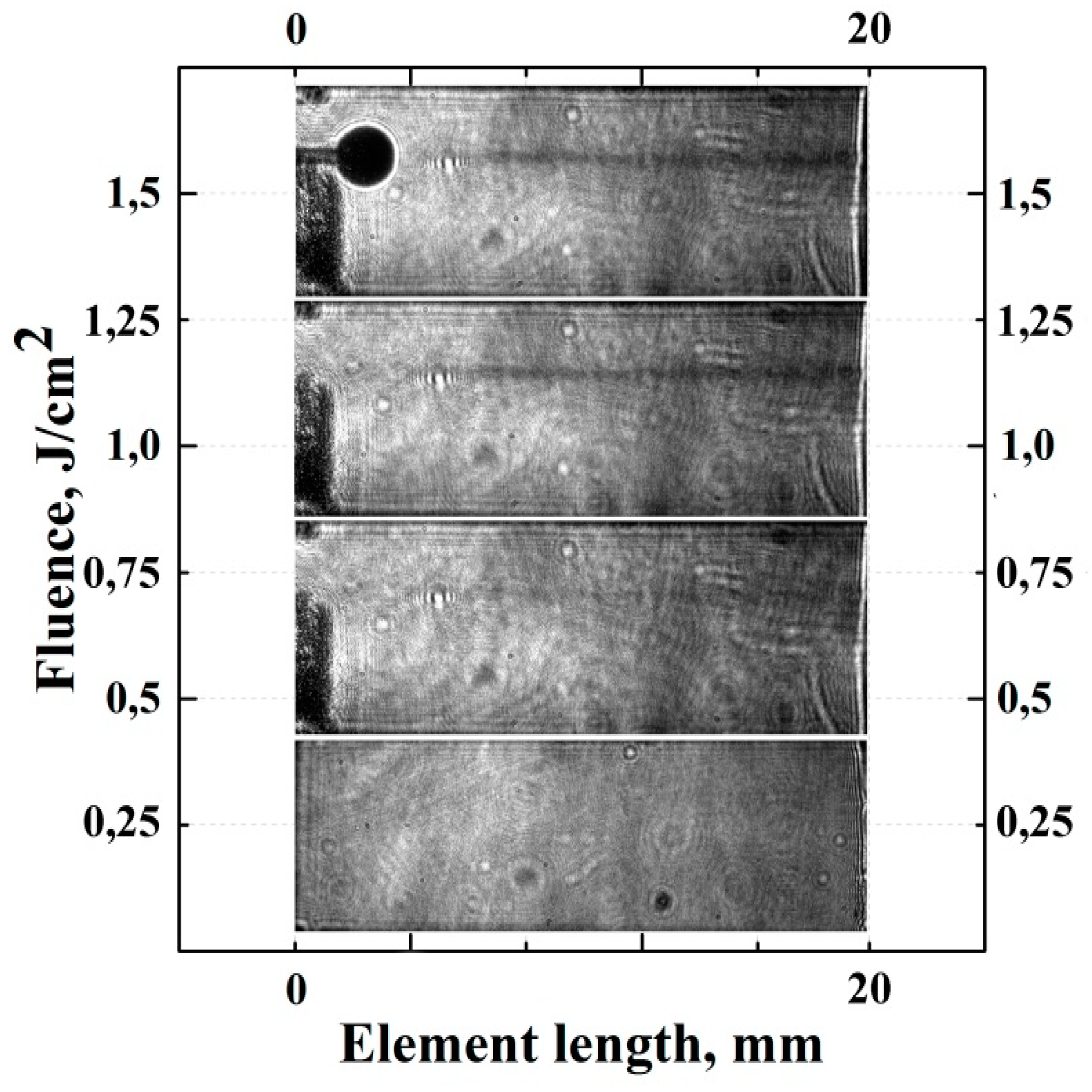
Figure 20 shows the restored holograms. At a power of up to 0.7 J/cm
2, the holographic camera didn’t detect any changes. With an increase of the pump fluence from 0.7 to 0.9 J/cm
2, the formation of a dark area along the entire length of the crystal was observed. With an increase of the fluence to 1.2 J/cm
2, this area became darker. At a power more than 1.2 J/cm
2 a damage track inside the ZGP element was registered.
Analysis of the dependencies presented in
Figure 16,
Figure 17,
Figure 18 and
Figure 19 and the dark tract images on the
Figure 20 allows us to conclude that the ZGP transmission decreases near the LIDT (above the pump fluence of 1 J/cm
2). With a decrease in PRR at the same average power (and an increase of the pumping pulse fluence), this dependence becomes more pronounced. These dependencies can be explained an induced nonlinear absorption near the LIDT (below the LIDT), which increased with the growth of the pumping pulse fluence. The nonlinear absorption can gave an additional contribution to the ZDP optical damage.
Further studies, which were carried out with the pumping fluence of 0.9 J/cm2 (which was two times less than the ZGP LIDT), the stable OPO operation was registered during more 6 minutes (this operation time was limited only by a thermal management of the system). If the pump fluence was more than 1.3 J/cm2, when the darkening was observed, the OPO operation time was limited by the LID that occurred after 30 seconds.
7. Conclusions
The paper presented up-to-date information on the initiation of LID inside ZGP single crystals under 2-μm Ho3+:YAG nanosecond laser irradiation and methodology for increasing the ZGP LIDT. The main findings are as follows:
1) It has been shown that an order of magnitude reduction in the number of bulk defects and dislocation concentration inside ZGP crystal increased the LIDT by more than three times.
2) It has been shown that the diffusion doping of ZGP single crystals with Mg and Se leads to higher LIDT. After annealing at 750 °C, the destruction threshold of samples doped with Mg and Se increased by 31% and 21% from 2.2 ± 0.1 J/cm2 to 2.9 ± 0.1 and 2.7 ± 0.1 J/cm2, respectively. The opposite trend was observed when ZGP was doped with Ca. A correlation was observed between the optical breakdown threshold and the electro-physical parameters of crystals after doping, in particular, when it comes to the conductivity of samples. A decrease in conductivity was observed when ZGP samples were doped with Mg and Se, while the conductivity of ZGP increased after doping with Ca compared to an undoped annealed sample. Studies have shown that there is a technological possibility to increase the LIDT of ZGP crystals by reducing the conductivity of samples using controlled doping.
3) An increase in the LIDT has been found after applying an AR coating. In the case of a coating based on ZnS and Al2O3 materials, the LIDT increased by 55% compared to an uncoated sample. It was assumed that there are no local composition fluctuations and mechanical stress in the layers of the transparent coating, which in turn leads to good adhesion of the multilayer coating to the polished surface of the crystal and increases the LIDT compared to the uncoated sample by closing the broken chemical bonds and bulk defects that have come out on the polished surface.
4) Data has been obtained on the dependence of the LIDT fluence on the laser beam diameter and intensity, the PRR, and the exposure.
5) A strong dependence of LIDT at 2.1 μm on the crystal temperature has been found. The observed sharp increase in the threshold energy density (up to 3 times the initial value) when the ZGP temperature was reduced from 0 °C to - 60 °C can be explained by the temperature dependence of the filling number of phonons. The increase in the filling number of phonons with a decrease in the temperature of the crystal leads to a decrease in the probability of their participation in indirect electron transitions from the valence band to impurity levels, and, accordingly, to a decrease in the nonlinear absorption of the crystal.
6. Visualization of the optical damage dynamics using digital holography showed the formation of an optical pre-damage track along the laser beam. The process of solidification of the molten material leads to the diffusion of free charge carriers from the heated region of the crystal in the direction perpendicular to the laser beam. The effect above the LIDT is accompanied by the appearance of a luminous spot near the exit optical surface inside the crystal and the subsequent movement of this luminous spot towards the input optical surface, i.e. in the direction opposite to the propagation of laser radiation. This luminous spot can be explained by the recombination of the formed non-equilibrium charge carriers.
7. Using a digital holographic camera, it was found that the pulsed beam intensity greater than or equal to the LIDT of the crystal leads to elastic deformations of the crystal in the longitudinal direction at the moment of formation of the damage track. These deformations were attributed to the thermal expansion of material in the damage track area, caused by a sharp increase in the local temperature along the laser beam to values exceeding the melting temperature of the crystal.
8. The presence of the reversible "photo darkening" area along the propagation path of a powerful laser beam at 2.1 μm in ZGP below the LIDT has been established. Such reversible photo darkening of the propagation channel can be explained by the local decrease in the band gap width of ZGP due to heating.
9. Over the course of studying the energy characteristics of the OPO based on a ZGP crystal and using the results of visualization of the processes taking place inside the crystal, we established that when the pump intensity reaches half the LIDT threshold the OPO efficiency stops growing and the darkening of the beam path inside the crystal starts forming. These effects were accompanied by the decrease in transmission when the crystal was irradiated outside the resonator, which may indicate significant nonlinear absorption. The results indicate that these processes are interrelated. The nonlinear absorption may be the cause of the decrease in the efficiency of parametric conversion and can be a factor that initiates the optical damage.
10. This review shows the significant potential for increasing LIDT ZGP by improving the structural perfection of the crystal and improving the quality of crystal surfaces by improving the technology of crystal growth, post-growth processing, polishing and AR of working surfaces.
