Submitted:
05 November 2024
Posted:
06 November 2024
Read the latest preprint version here
Abstract
I report on the first observed self-amplification by stimulated emission of 0.2THz and 1.63THz radiation using InGaAs/GaAs HEMT operating in the deep saturation regime at room temperature. I demonstrate both theoretically and experimentally that the Sub-THz and THz FETs response is due to rectification of the nonlinear dependence of the device current-voltage characteristics. FETs do operate as a nonlinear THz mixers and rectifiers and its open-drain responsivity is given by a similar expression to that of zero-bias Schottky diode detector. However, operating FETs deep in the saturation regime does allow the accurate tuning of the device to the resonance condition or the negative resistance mode at room temperature, hence FETs can be tuned in the deep saturation regime to enable sub-THz and THz lasing effect. This observed sub-THz and THz laser phenomena using FETs will revolutionize human technology in all fields of life in the near future.
Keywords:
terahertz electronics
; laser
; negative resistance
; plasma instability
; room temperature
; resonance
; millimeter wave
; THz rectifiers
Field effect transistors (FETs) and high electron mobility transistors (HEMTs) in different technologies and material systems have been explored for terahertz detection since long time ago. The exploration of plasma oscillations phenomena in field-effect transistors’ channel has begun long time ago starting from the theoretical prediction [1] that such waves have linear dispersion, , with the velocity controlled by the gate voltage swing . This work was followed by observation of infrared asbsorption [2] and weak infrared emission [3] related to excitation of plasma oscillations in silicon inversion layers.
In recent decades, the interest to plasma phenomena in FETs channels have increased due to realization that high typical values of () are promising for utilization of plasma oscillations in emission and detection of THz radiation [4,5]. Dyakonov and Shur have emphasized that an instability of charge carriers’ oscillations in transistor’s channel can occurs when dc current flow in the device channel and emit terahertz radiation, while the nonlinearity of the device allows detection and mixing in the terahertz range. However, this plasma instability was only observed at very low temperature and the studies were limited to open-drain or unbiased transistors since Dyakonov and Shur physical model was limited to this operation mode.
The research in this field of THz electronics [6,7,8,9,10,11,12,13,14,15,16,17,18,19,20,21,22,23,24,25,26] has led to resonant and broadband (non-resonant) detection or emission of sub-THz and THz radiation by nanoscale FETs. Though the THz emitters are still rather weak, the THz detectors already show good performance: they are tunable [6,7,8,9,10,11,12,13,14,15,16,17,18,19,20,21,22,23,24,25,26] by varying the gate voltage and the drain current, with fast response time [21] and demonstrate relatively low noise equivalent power (NEP) up to room temperature [18]. Hence, they are promising candidates for terahertz systems applications.
As shown in Refs. [6,17], the efficiency of the broadband detection can be significantly improved by applying drain current j to drive FETs into the saturation regime. The physical model [17] demonstrates that the response essentially increases when approaches the saturation current jsat; (knee current on I-V curve). However, THz response of FETs operating in the deep saturation regime, j>jsat, was neither investigated experimentally nor theoretically until this work.
I start with the theoretical discussion. At very small drain biasing voltages, the I-V characteristic of transistor can be written as , where is the channel conductivity depending on both gate-to-source and gate-to-drain voltages. The incident terahertz radiation will couple to transistor channel from both source and drain sides. Thus, an induced dc current will flow in the device, if an external load resistor is connected with the transistor, the latest dc current can be re-written as: , where the change in conductivity can be expressed as a function of effective variations in applied gate-to-source and gate-to-drain voltages: .
I can also express the radiation-induced drain to source voltage as: . Since the device is operating in the open drain condition with very small signal variations at both source and drain terminals, we can assume that , hence the induced dc terahertz response in the device can be given by:
One can consider two radiation-induced ac voltage sources and at transistor source and drain terminals, respectively. Thus, the effective dc variations in gate-to-source and gate-to-drain voltages are given by: and . So, Equation (1) explains why the response can be positive or negative based on the ratio of , this ratio is mainly determined by the metallization layout of transistor terminals. For open-drain detection, coupling of terahertz radiation will be distorted unless a special attention is considered for the design of transistor layout.
By neglecting the external load effect from Equation (1), the intrinsic THz responsivity of open-drain transistor can be expressed as a function of the device I-V characteristic in a similar way to that of zero-bias Schottky diode detector. For transistor, THz responsivity is given by:
while for a Schottky diode detector it is written as:
and this confirms that the mechanisms of terahertz detection in both devices are the same, due to the rectification of the nonlinear behavior of their current-voltage characteristics. However, transistor has the advantage that its detectivity is tunable by the applied gate voltage.
One should notice that the THz response of FETs given by Equation (1) is valid for gate-bias voltages both above and below the transistor threshold voltage. For the regime above the threshold, we can easily find from drain current equation that: . In such a case, an approximate behavioral expression for the response can be written as:
As for the sub-threshold regime, since the transistor drain current is proportional to and , where is the sub-threshold ideality factor and is the thermal voltage. One can find that: , and another simplified behavioral equation for terahertz response at gate biasing below the threshold voltage can be obtained as:
In the case of drain-biased transistors, I can also approximately express the induced THz radiation voltage across the transistors drain and source terminals as: therefore an approximate behavioral expression for the induced dc terahertz response using the transistor’s transconductance can be written as:
Here I show for the first time that for j > jsat a further dramatic growth of broadband response can be achieved. I report that in this region response continues to grow linearly with dc drain voltage (or dc drain current) and it may reach very high values. The THz rectification in the deep saturation operation regime has a tremendous importance for THz electronics and it is the key solution for tuning the device into the negative resistance resonance mode or in other words the sub-THz and THz lasing effect at room temperature. I don’t exaggerate if I say that the result of this research will change the world.
In order to explain how the self-amplification by stimulated emission at Sub-THz and THz frequencies can be observed in the FETs channels, let’s consider the following simple example: the resonance of any sound wave in a tube is function of three main parameters: the frequency of the wave, the length of the tube, and the density of particles in the tube. Unfortunately, researcher in the field of THz electronics focused their attention for long time only at the open-drain FETs operation regime. At zero drain-biased mode, the conductivity of the transistor’s channel is almost uniform and the hydrodynamic equations from device physics (Euler and Continuity) can be solved and gives a closed solution formula. On the contrary, the drain-biased channel conductivity is not uniform at all and the hydrodynamic equations cannot be solved analytically and only the numerical solver can find a solution without any closed form formula.
The main challenge to achieve THz plasma resonance in the open-drain operation mode is that the length of the channel is always fixed and equal to the physical distance of the transistors gate [4,5], since the minimum gate length is currently above 20nm in the commercial technology at the year of 2010.
Therefore, it is only possible to tune the THz frequency of the input radiation to achieve the negative resistance resonance on a fixed transistor channel length. So far it is very hard to tune the frequency of the commercially available THz sources, therefore the plasma wave THz emitters are still rather weak and are limited for some THz frequencies at the lower millimeter wave range.
Some THz electronics’ researchers focused for long time on the very low operation temperature to almost freeze the transistor channel to both reduce and tune its channel resistance to lower values which can achieve resonance with longer devices, and they used cascaded design to overcome the weak resonance mode by amplifying the output THz radiation as much as possible. However, the very low temperature needed for quantum cascade THz lasers [27] limits its mass volume technology applications at few limited sub-THz frequencies
The key solution presented in this research that will enable tunable room temperature lasing effect at wide range of sub-THz and THz frequencies is operating the FETs and HEMTs in the deep saturation regime. As shown in Figure 1, the effective channel length is tuned by varying the applied drain to source voltage, therefore the negative resistance resonance mode can occur independent of any transistor gate size.
Next, I discuss my experimental data. I used 0.5μm enhancement mode InGaAs/GaAs pseudomorphic HEMTs fabricated by TriQuint Semiconductor as terahertz detectors, all its important device parameters are extracted in Ref. [26]. The optically pumped far-infrared gas laser (Coherent SIFIR-50) was utilized as a terahertz source operating at 1.63THz. The laser beam was focused on the transistor using polyethylene lens with focal length of 16mm and modulated by an optical chopper with a fixed frequency of 50 Hz. The induced dc drain voltage superimposed on the drain-to-source voltage was measured using the lock-in amplifier SR-830.
Figure 2 shows both the open-drain and drain-biased responsivity curves obtained by firstly tuning the gate-to-source bias for the open-drain case at different load resistances and then compare it with the simplified physical model of Equation (1), then secondly by tuning the drain-to-source current for a fixed gate bias and fixed load resistance =10K Ohm and then compare it with Equation (7).
It worth mentioning that all the above results do only show the nonlinear-rectification of THz radiation at the transistors source and drain terminals at higher frequency much beyond the cutoff frequency. There is no observation yet of plasma resonance or negative resistance lasing effect for different bias conditions. The reason for missing the resonance condition is that the length of the device and its conductivity doesn’t match the higher frequency of 1.63THz yet.
I here propose an alternative method instead of freezing the device at very low operation temperature. By operating the transistor in the subthreshold region, it is possible to reduce the channel resistivity to its possible minimum values, then finally one can drive the FET under test into the sub-threshold and the deep saturation regime simultaneously. Therefore, it is possible to tune the channel length and conductivity to match the resonance condition at very high frequency radiation at room temperature.
Figure 3 shows for the first time ever in the world (for the best of my knowledge) the experimental physics observation of plasma instability, negative resistance, or THz resonance condition in a long FET (0.5um technology) device above one THz at room temperature.
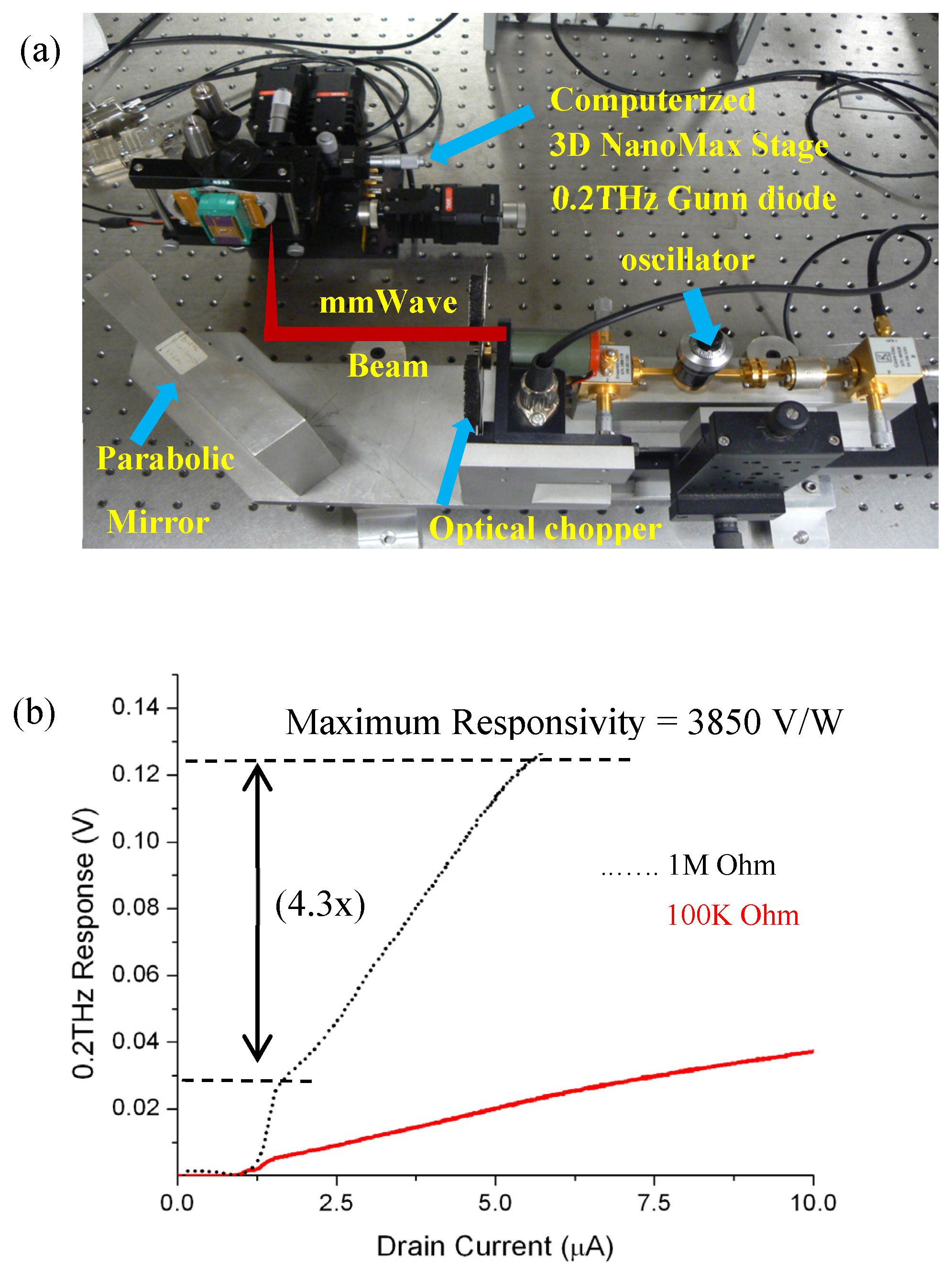
In order to justify the strong plasma instability at room temperature with a long transistor device, I have tested the same fabricated HEMTs under the illumination of the focused 200GHz radiation beam generated from a commercial Gunn diode oscillator (see Figure 4). The optical chopper was set to 50Hz modulation frequency. The computerized 3D NanoMax stage was used to allocate the FET device on the best focused area of the radiation beam. The THz responsivity at 200GHz was at least an order of magnitude higher than that at 1.63THz (up to 170V/W). I do report a responsivity as high as 3850V/W at 200GHz without the need of any integrated coupling antenna, while the current waveguide-based Schottky diode detector from Virginia diodes, Inc [28] does show THz responsivity of 4000V/W.
The nonlinearity 0.2THz rectification response with the emphasize on the linear growth in the transistor’s response appears clearly in Figure 4(b) within the deep saturation regime. One can observe that THz responsivity can be increased by 2-4 times when transistors operate deeper in the saturation regime and an additional increase in responsivity may be gained when many transistors are connected in series [26]. Also, it worth mentioning here that deep saturation regime can be used for imaging the incident THz radiation at sub-wavelength resolution (up to 1/10 times than the radiation wavelength) as shown in Refs. [25].
Figure 4.
(color online) (a) Experimental setup for studying the 200GHz millimeter wave direct coupling with the designed transistors test structure. (b) Measured 0.2THz response as a function of drain-currents for different load resistances. The HEMT transistor is biased in the sub-threshold regime with gate-to-source voltage of 0.25V.
I do empathize that the noise equivalent power (NEP) in the case of deep saturation operation regime may be much higher than that of the Schottky diode detector due to the high drain current in the device. However, there are multiple options to reduce the NEP of the FETs power THz detectors. First one is to bias transistor in the sub-threshold regime where the drain current is the minimum while the responsivity is still at very high values, second one is to connect the transistors in series and the signal-to noise-ratio (SNR) can be improved by a factor of for the series connection of many transistors in the saturation regime [26], where N is the number of connected transistors. In addition, the electronic modulation of incident THz radiation above the 1/f corner frequency can also enhance the SNR [19].
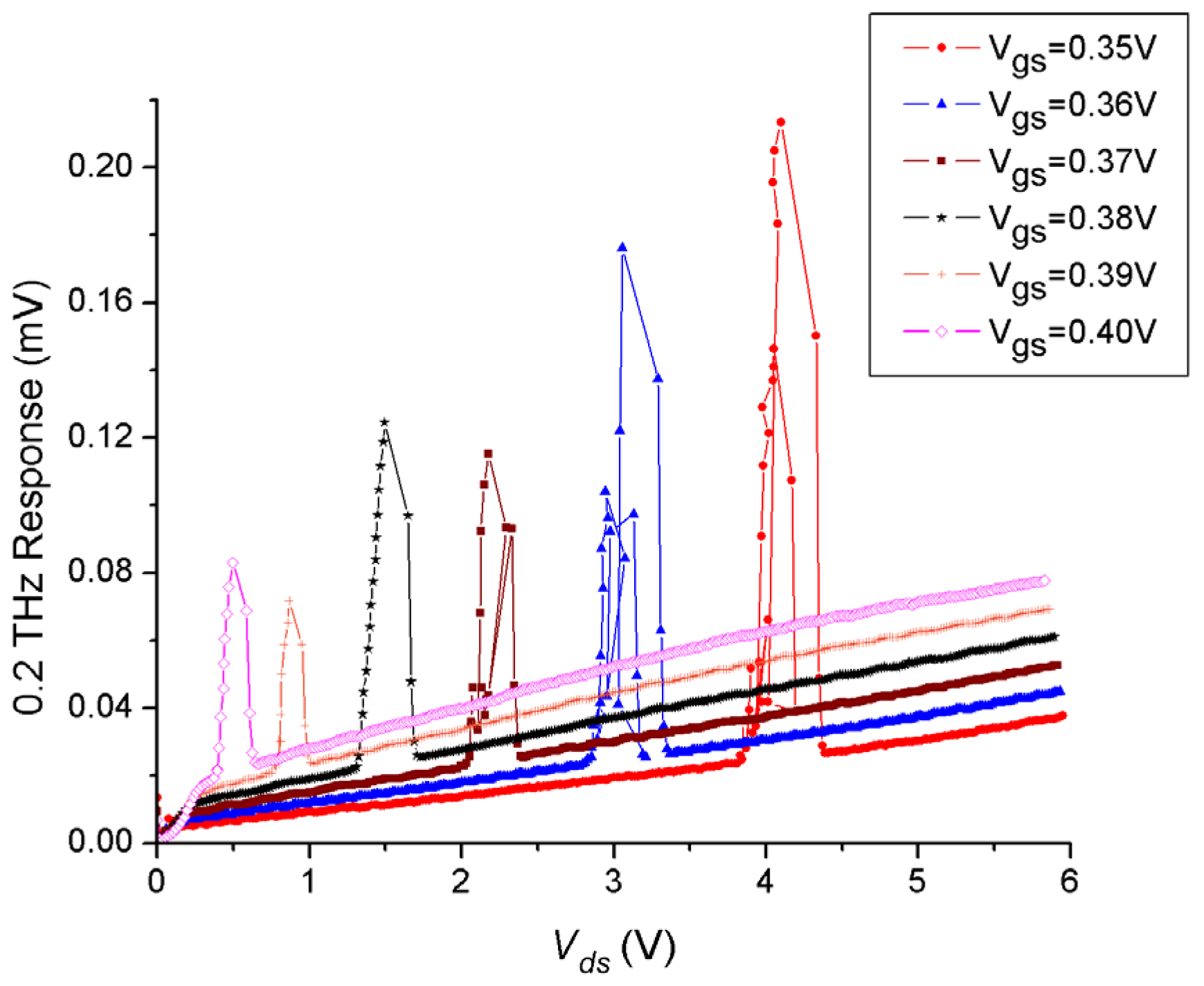
In addition to the high 0.2THz responsivity presented above, I was able to successfully tune both the gate-to-source and drain-to-source biasing conditions to observe very strong plasma instability at 200GHz at room temperature. Figure 5 presents for the first time ever (for the best of my knowledge) multiple plasma instability and self-amplification by stimulated emission of 200GHz radiation. Although there is no specific analytical solution to describe the plasma instability under this non-uniform distributed channel resistivity, only numerical simulation can solve and justify these experimental physics observations. However, these experimental results were verified by many different samples that can give us the same results each time.
One can easily analyze the THz response in Figure 5 and come up with the following indications: For the highest gate-to-source values, the resistivity of transistor channel is minimum and instability reach maximum peak with highest drain-to-source value. In other words, the less the channel resistivity the shorter the effective channel length L* is needed to achieve the strongest negative resistance instability condition. On the other hand, the non-linearity rectification response is the least due to the lower amplification factor at higher Ugs values. One can conclude also that this negative resistance instability can be tuned for different Sub-THz frequencies like 210GHz and 195GHz very easily because the effective channel length L* can be simply tuned by Uds. The operation of the FETs and HEMTs THz detector and emitters in the deep saturation regime opened the opportunity for the world to fine tune sub-THz, THz, and infrared lasing effect at room temperature over wide range of frequency range with the smallest possible frequency steps.
Finally, I should mention that using the nonlinearity of FETs and HEMTs as single device, as one-dimensional array, as two-dimensional array, or as series connected devices for rectification, mixing, power detection, or high frequency radiation imaging or sensing is much better choice when compared to the classical Schottky diode detector. However, the operation of a single FET in the negative resistance resonance mode will always demonstrate instability when it is fine-tuned by both gate-to-source and drain-to-source and then adding the proper load resistance. Therefore, I do suggest to use the differential mode FETs structure as the one I have designed and tested [25] to stabilize the plasma instability resonance and obtain stable Sub-THz and THz sources that can operate very well with high power and high frequencies at both room temperatures and at very low temperatures such as in the satellite communication systems
In conclusion, I have justified both theoretically and experimentally that terahertz detection using field effect transistors is due to rectification of the nonlinear properties of its current-voltage characteristic, the same mechanism as for Schottky diode THz detector. I have also illustrated that terahertz radiation does couple directly to transistor channel via both source and drain terminals and not through its gate, and that explains why transistor is capable of detection at much higher frequency beyond its cut-off frequency. I have demonstrated for the first time the experimental realization of strong self-amplification by stimulated emission of sub-THz and THz radiation using HEMTs operating in the deep saturation regime at room temperature.
Briefly, I do expect that this reported results here will revolutionize human technology in all domains of life. For example: (a) it will enable much high frequency wireless communications on ground and between satellites at very high speeds and data rates much beyond 3G and 4G, (b) it will allow very high clock speeds for computer’s central processing unit (CPU) and Graphical processing unit (GPU) and all data servers, (c) it will realize new kind of energy weapons like microwave guns but with additional option of frequency tuning with much higher output power and much smaller equipment’s sizes, (d) it will provide high resolution sub-wavelength THz imaging for many different life applications, (e) it will ease the electronics communication with the human brain and the detailed study of brain activities, (f) it will significantly improve THz astronomy and the environmental climate monitoring and controlling technology, (g) it will make the non-destructive analysis of materials and electronics devices much easier. In summary, why not change the world? as the logo of Rensselaer Polytechnic Institute (RPI) states.
This work was only sponsored by the graduate scholarship of RPI (to the best of my knowledge) for me as a research assistant, all the results were obtained in the labs of the center of terahertz research in RPI. I would like to thank all my colleagues at the center of terahertz research for helping me and guiding me to use the complicated lab equipment in the center. Finally, I would like to thank Allah (my Lord) the creator of the universe for inspiring me to do this research and allowing me to learn new physics in the world made by Allah, and I hope this new physics will help the world to be a better place. This manuscript was prepared on march 29th, 2010. I will put it on hold and hide it for political reasons due to its national security issues which make it highly classified material.
References
- 1A.V. Chaplik, Zh. Eksp. Teor. Fiz., 62, 746 (1972) [Sov. Phys. JETP 35, 395 (1972)].
- 2 S.J. Allen, Jr., D.C. Tsui, and R.A. Logan, Phys. Rev. Lett. 38, 980 (1977).
- 3 D.C. Tsui, E. Gornik, and R.A. Logan, Solid State Comm. 35, 875 (1980).
- 4M. Dyakonov and M. S. Shur, Phys. Rev. Lett. 71, 2465 (1993).
- 5M. Dyakonov and M. S. Shur, IEEE Trans. on Elec. Dev. 43, 380 (1996).
- 6J-Q. Lu and M.S. Shur, Appl. Phys. Lett. 78, 2587 (2001).
- 7W. Knap, V. Kachorovskii, Y. Deng, S. Rumyantsev, J.-Q. Lu, R. Gaska, M. S. Shur, G. Simin, X. Hu and M. Asif Khan, C. A. Saylor, L. C. Brunel, J. of Appl. Phys. 91, 9346 (2002).
- 8W. Knap, Y. Deng, S. Rumyantsev, and M. S. Shur, Appl. Phys. Lett. 81, 4637 (2002).
- 9W. Knap, Y. Deng, S. Rumyantsev, J.-Q. Lü, M. S. Shur, C. A. Saylor, and L. C. Brunel, Appl. Phys. Lett. 80, 3433 (2002).
- 10T. Otsuji, M. Hanabe, and O. Ogawara, Appl. Phys. Lett. 85, 2119 (2004).
- 11W. Knap, F. Teppe, Y. Meziani, N. Dyakonova, J. Łusakowski, F. Boeuf, T. Skotnicki, D. Maude, S. Rumyantsev, and M. S. Shur, Appl. Phys. Lett. 85, 675 (2004).
- 12Y. Deng, M. S. Shur, R. Gaska, G. S. Simin, M. A. Khan, and V. Ryzhii, Appl. Phys. Lett. 84, 70 (2004).
- 13F. Teppe, W. Knap, D. Veksler, M. S. Shur, A. P. Dmitriev, V.Y. Kachorovskii, and S. Rumyantsev, Appl. Phys. Lett. 87, 052107 (2005).
- 14F. Teppe, M. Orlov, A. El Fatimy, A. Tiberj, W. Knap, J. Torres, V. Gavrilenko, A. Shchepetov, Y. Roelens, and S. Bollaert, Appl. Phys. Lett. 89, 222109 (2006).
- 15A. El Fatimy, F. Teppe, N. Dyakonova, W. Knap, D. Seliuta, G. Valušis, A. Shchepetov, Y. Roelens, S. Bollaert, A. Cappy, and S. Rumyantsev, Appl. Phys. Lett. 89, 131926 (2006).
- 16R. Tauk, F. Teppe, S. Boubanga, D. Coquillat, W. Knap, Y. M. Meziani, C. Gallon, F. Boeuf, T. Skotnicki, C. Fenouillet-Beranger, D. K. Maude, S. Rumyantsev, and M. S. Shur, Appl. Phys. Lett. 89, 253511 (2006).
- 17D. Veksler, F. Teppe, A. P. Dmitriev, V. Yu. Kachorovskii, W. Knap, and M. S. Shur, Phys. Rev. B 73, 125328 (2006).
- 18W. J. Stillman and M. S. Shur, J. of Nanoelectronics and Optoelectronics. 2, 209 (2007).
- 19D. Veksler, A. Muravjov, W. Stillman, Nezih Pala, and M. Shur, Proc. 6th IEEE sensors Conf. (Atlanta, GA, USA 2007), pp.443.
- 20S. Boubanga-Tombet, F. Teppe, D. Coquillat, S. Nadar, N. Dyakonova, H. Videlier, W. Knap, A. Shchepetov, C. Gardès, Y. Roelens, S. Bollaert, D. Seliuta, R. Vadoklis, and G. Valušis, Appl. Phys. Lett. 92, 212101 (2008).
- 21V. Yu. Kachorovskii and M. S. Shur, Solid-State Electronics. 52, 182 (2008).
- 22S. Boubanga-Tombet, M. Sakowicz, D. Coquillat, F. Teppe, W. Knap, M. I. Dyakonov, K. Karpierz, J. Łusakowski, and M. Grynberg, Appl. Phys. Lett. 95, 072106 (2009).
- 23D. B. Veksler, V. Yu. Kachorovskii, A. V. Muravjov, T. A. Elkhatib, K. N. Salama, X.-C. Zhang, and M. S. Shur, Solid State Electronics, 53, 571 (2009).
- 24T. A. Elkhatib, V. Y. Kachorovskii, A.V. Muravjov , X.-C. Zhang, and M. S. Shur, Proc. 36th Inter. Symp. On Compound Semiconductors, (Santa Barbara, CA, USA, 2009), pp.263.
- 25T. A. Elkhatib, A. V. Muravjov, D. B. Veksler, W. J. Stillman, V. Y. Kachorovskii, X.-C. Zhang, and M. S. Shur, Proc. 8th IEEE sensors Conf. (Christchurch, New Zealand, 2009), pp.1988.
- 26T. A. Elkhatib, V.Yu. Kachorovskii, W. J. Stillman, D. B. Veksler, K. N. Salama, Xi-C. Zhang, and M. S. Shur,” IEEE Trans. on Microwave Theory and Technique, 58, 331 (2010).
- 27G. Scalari, C. Walther, M. Fischer, R. Terazzi, and H. Beere, D. Ritchie, J. Faist. Laser & Photonics Reviews, 3, 1-2 (2009).
- 28www.virginiadiodes.com.
Figure 1.
(color online) Schematic of the channel of field effect transistor operating in the deep saturation regime. The plasma resonance oscillations happen when the effective channel length L* is tuned to match the incident radiation frequency.
Figure 1.
(color online) Schematic of the channel of field effect transistor operating in the deep saturation regime. The plasma resonance oscillations happen when the effective channel length L* is tuned to match the incident radiation frequency.
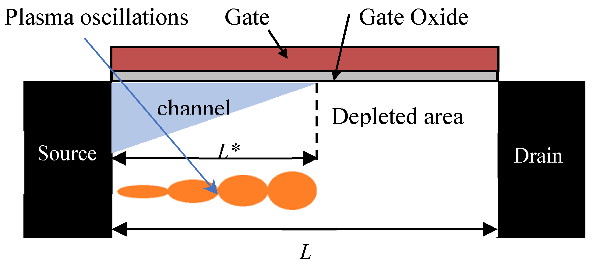
Figure 2.
(color online) Measured and calculated 1.63THz response as a function of: (a) gate-biases for the open-drain case in a semi-log scale, (b) drain-currents for the drain-biased case with a load resistance of 10K Ohm. The circuit diagrams for each case are shown within the responsivity curves.
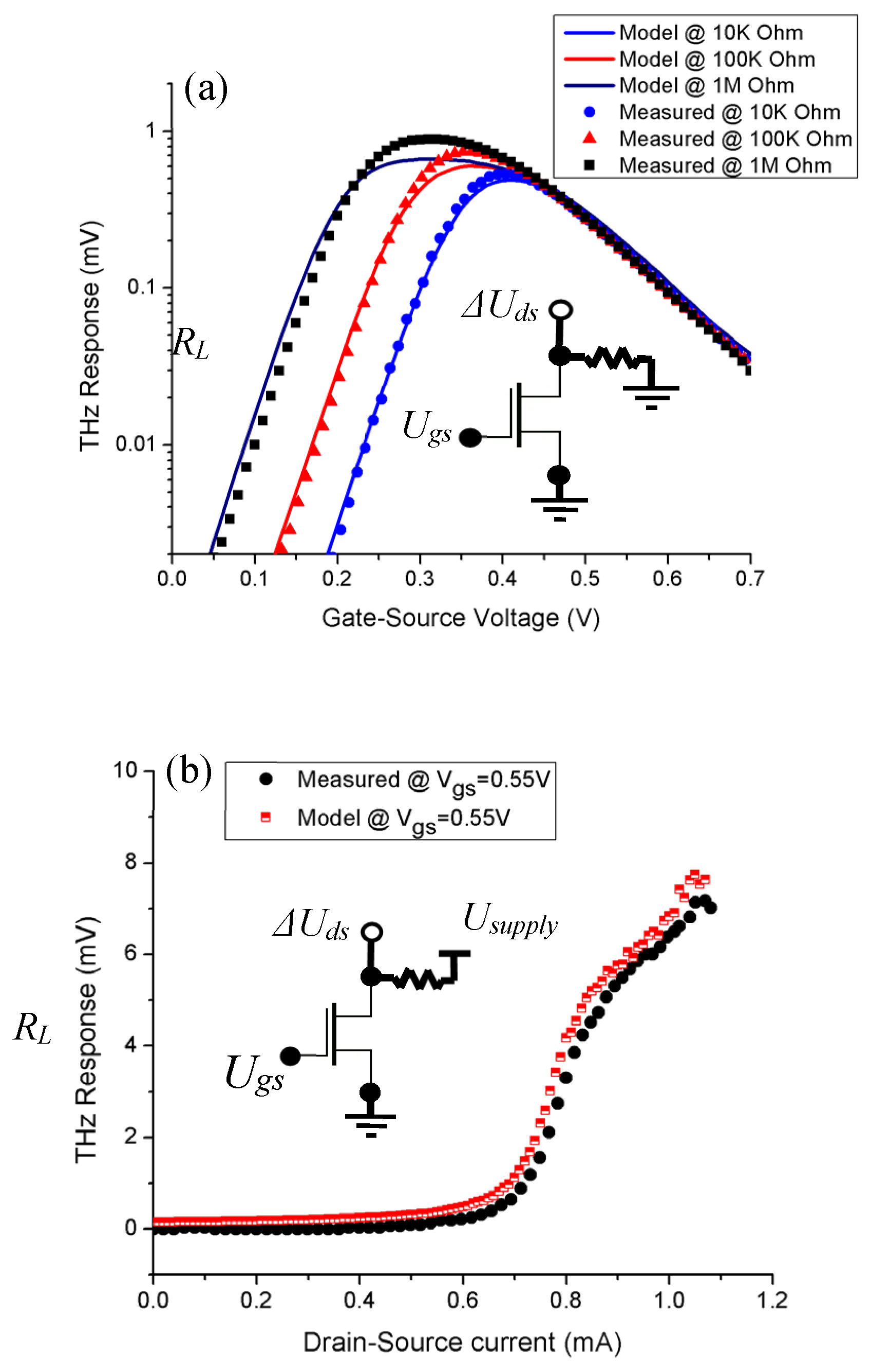
Figure 3.
(color online) Measured 1.63THz response as a function of drain-currents for the drain-biased case with a load resistance of 100K Ohm in a log-log plot. The first ever observed room temperature weak plasma instability or negative resistance resonance appears using InGaAs/GaAs 0.5um HEMTs at a sub-threshold gate-to-source bias of 0.25V and drain current of about 1μA deep in the saturation regime.
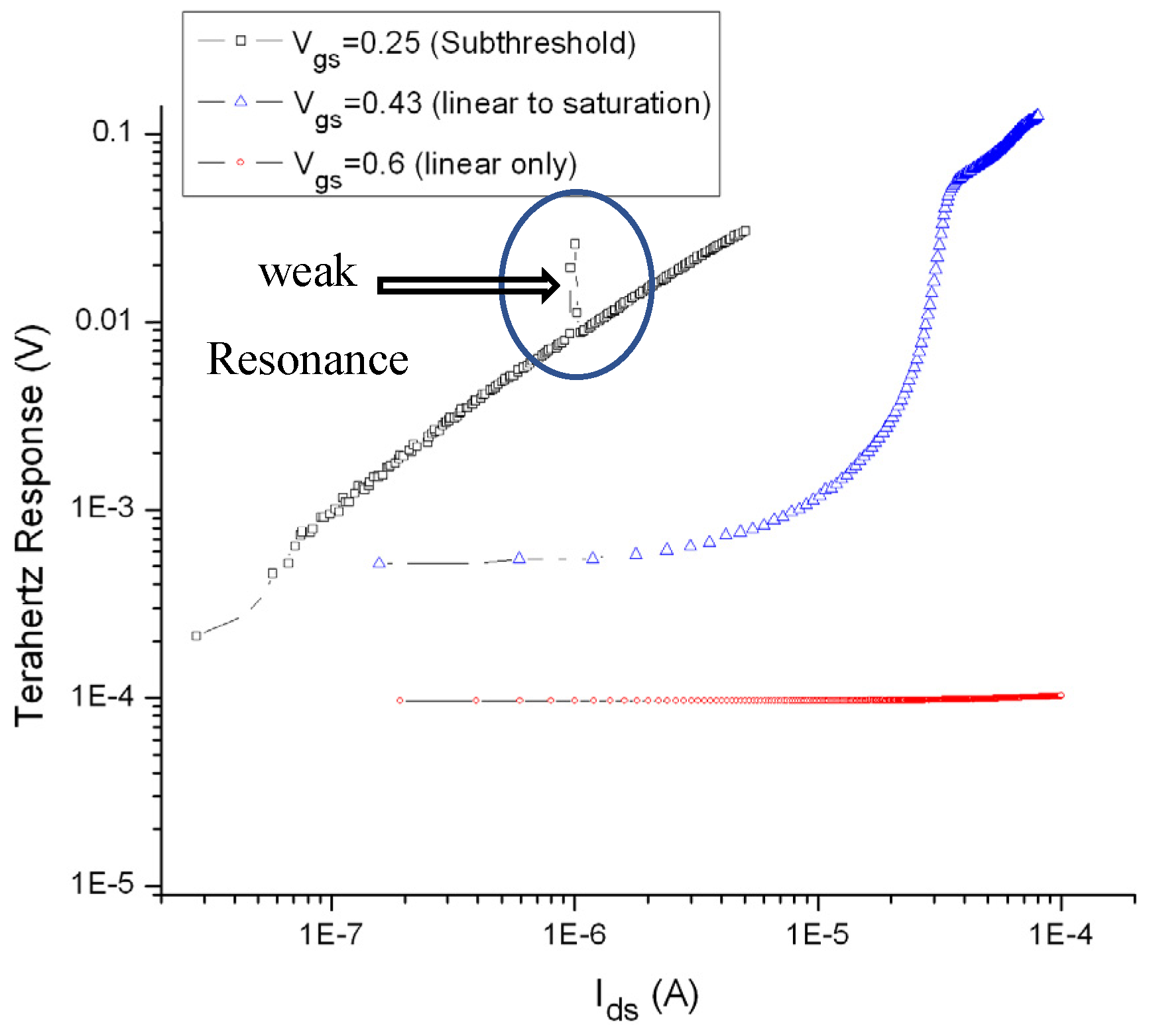
Figure 5.
(color online) Measured 0.2THz response as a function of drain-to-source voltages for a load resistance of 100K Ohm. The instability of carrier oscillations and the self-amplifications by stimulated emission appears clearly as unexpected peaks at different gate-to-source voltages and drain-to-source biasing.
Disclaimer/Publisher’s Note: The statements, opinions and data contained in all publications are solely those of the individual author(s) and contributor(s) and not of MDPI and/or the editor(s). MDPI and/or the editor(s) disclaim responsibility for any injury to people or property resulting from any ideas, methods, instructions or products referred to in the content. |
© 2024 by the authors. Licensee MDPI, Basel, Switzerland. This article is an open access article distributed under the terms and conditions of the Creative Commons Attribution (CC BY) license (http://creativecommons.org/licenses/by/4.0/).
Copyright: This open access article is published under a Creative Commons CC BY 4.0 license, which permit the free download, distribution, and reuse, provided that the author and preprint are cited in any reuse.


